Unlocking Superior Performance with High Frequency Laminate PCB
In the fast-paced world of electronics, the high frequency laminate PCB stands out as a cornerstone for cutting-edge applications. This specialized circuit board, crafted from advanced materials, ensures seamless signal transmission at elevated frequencies, making it indispensable for modern devices. At hcdpcba, we pride ourselves on delivering these innovative solutions that blend precision engineering with reliability, tailored to meet the demands of industries like telecommunications and automotive electronics.
Understanding the Essence of High Frequency Laminate PCB
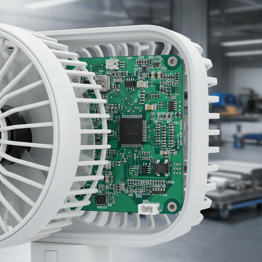
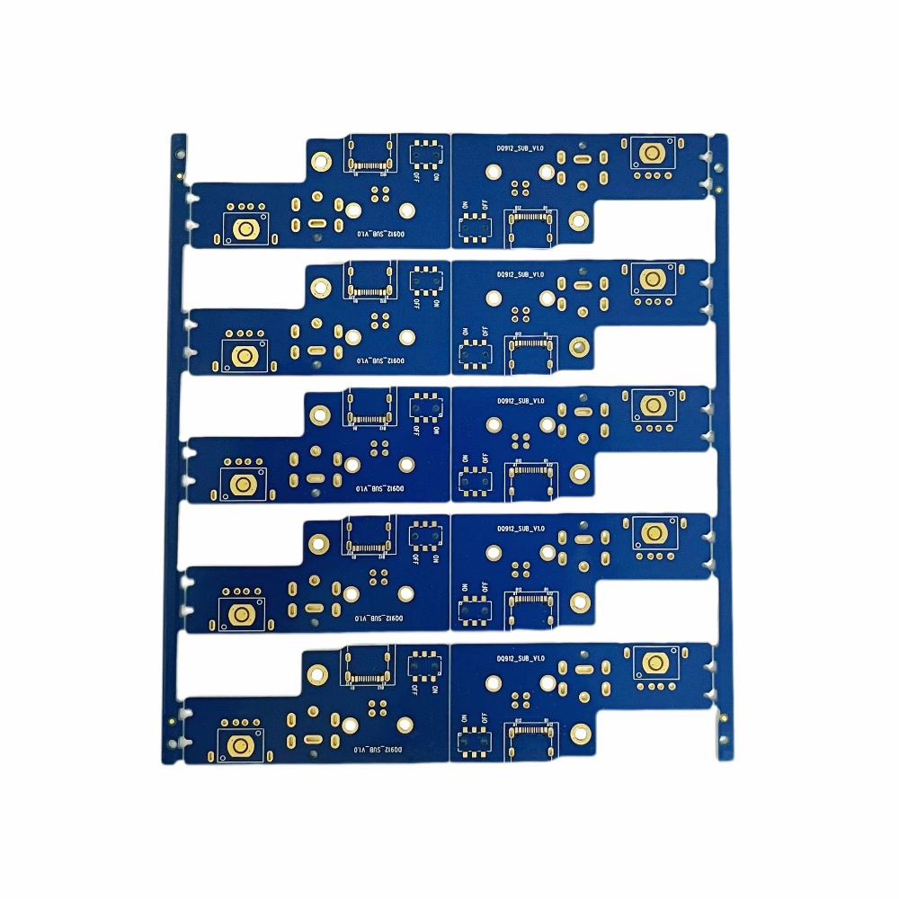
High frequency laminate PCB is engineered with substrates that offer exceptional electrical properties, minimizing signal loss and enhancing overall performance. Imagine a vibrant blue PCB panel, meticulously designed with a durable premium-grade substrate that withstands harsh environmental conditions while maintaining stability. Our product features a sleek solder mask that not only captivates the eye but also bolsters insulation, complemented by clear silkscreen labels for effortless assembly. The layout is optimized for signal integrity, with strategically placed vias and connectors that reduce interference and facilitate integration into complex systems. This versatility extends to a wide array of applications, from consumer gadgets to industrial controls, ensuring your projects thrive under high-speed operations.
Integrating RF Systems PCB for Advanced Connectivity
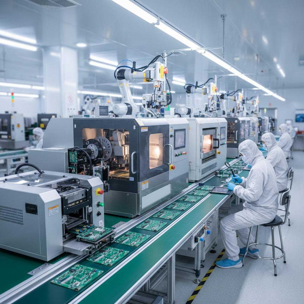
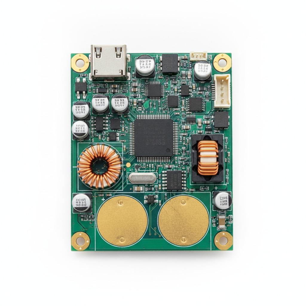
When it comes to RF systems PCB, the focus shifts to harnessing radio frequency signals with unparalleled efficiency. Our high frequency laminate PCB excels in this domain, providing the backbone for wireless communication devices that demand low latency and high throughput. Picture an intricately assembled board where every trace is calibrated to support RF modules without compromising on speed or clarity. At hcdpcba, our expertise in PCBA boards, including multi-layer and HDI variants, ensures that RF systems PCB are customized for sectors like IoT and smart home technologies. We offer comprehensive services such as SMT placement and component sourcing, guaranteeing that your RF-driven innovations are both functional and future-proof. The pre-designed mounting points on our panels simplify assembly, cutting down on production time and errors, while our DFMA analysis optimizes designs for cost-effective manufacturing.
Achieving Excellence with Low Dielectric Loss PCB
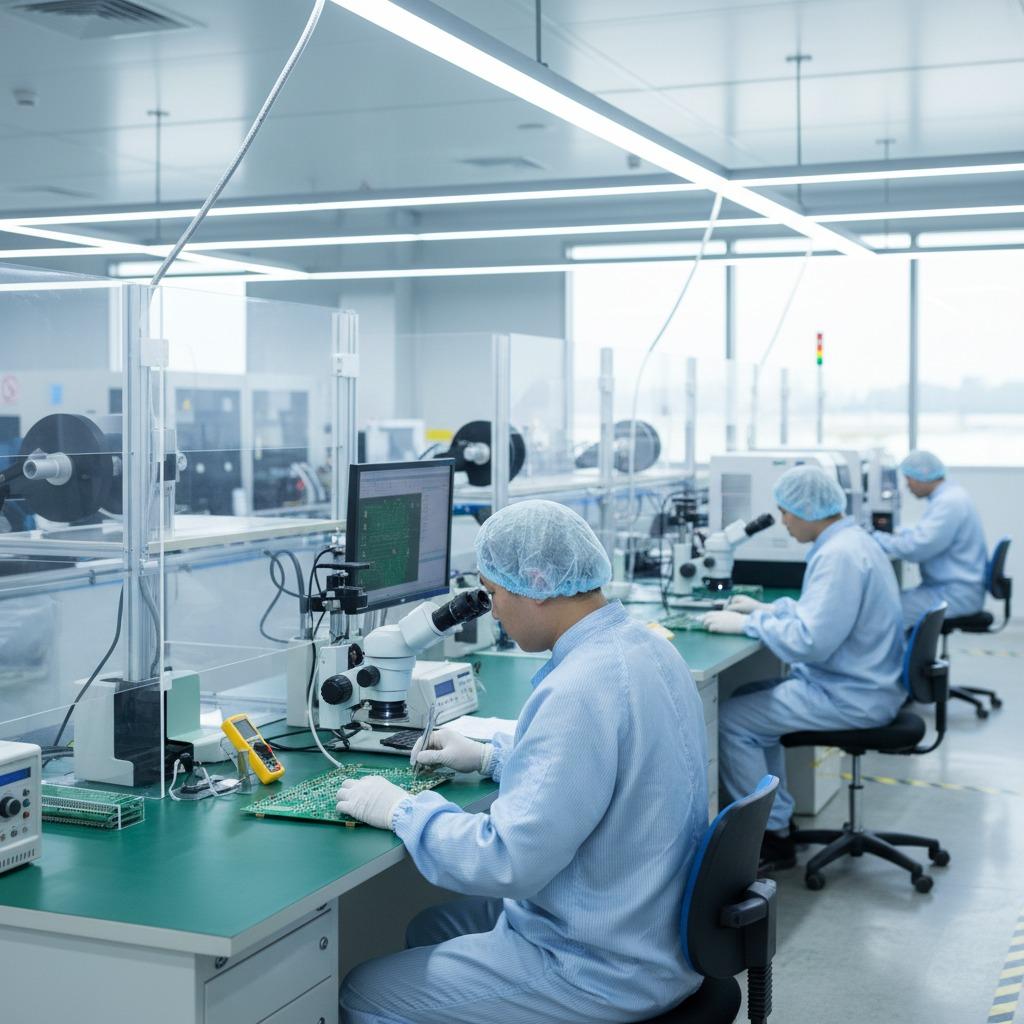
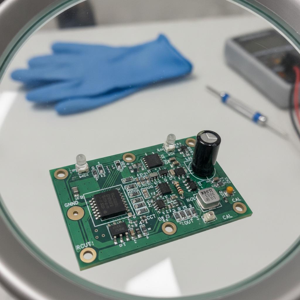
Low dielectric loss PCB is a critical feature in high frequency laminate PCB, where even the slightest energy dissipation can hinder performance. Our solutions minimize this loss through high-quality materials that preserve signal strength over long distances, ideal for applications in medical devices and power systems. Envision a board that not only looks striking in its blue hue but also performs flawlessly under rigorous testing, thanks to our stringent quality controls at hcdpcba. We specialize in rapid PCB prototyping and full-scale production, supporting small to large batches without engineering fees. Our OEM and ODM services allow for bespoke designs that align with your vision, backed by a team of seasoned professionals providing technical support and confidentiality agreements to safeguard your intellectual property. This commitment to low dielectric loss ensures that devices in communications and AI fields operate at peak efficiency, reducing heat and extending lifespan.
Why Choose hcdpcba for Your High Frequency Needs
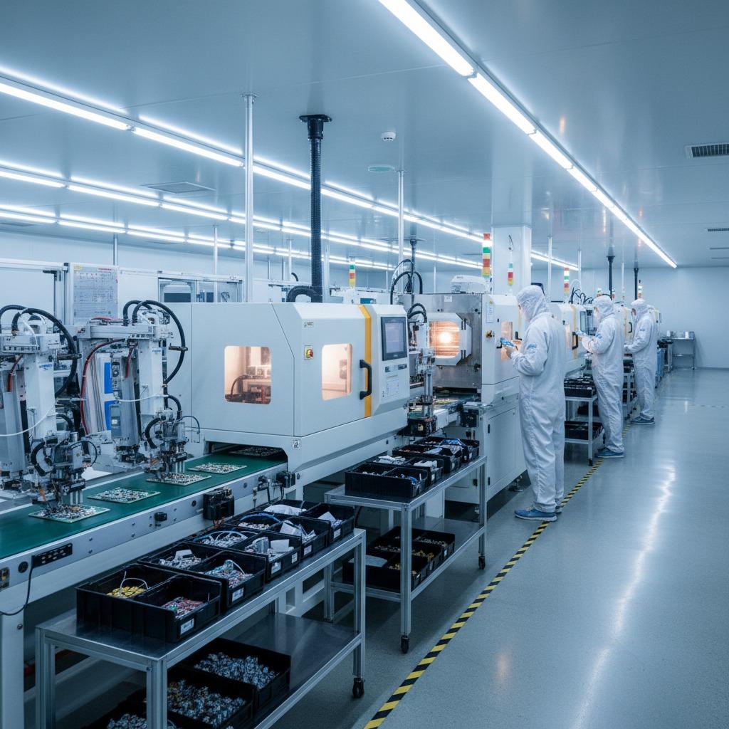
Partnering with hcdpcba means accessing a suite of services that elevate your projects beyond the ordinary. From efficient component procurement to thorough testing and assembly, we streamline the entire process to deliver zero-defect products. Our cost advantages stem from optimized workflows, enabling competitive pricing without sacrificing quality. Whether you're developing RF systems PCB or seeking low dielectric loss PCB solutions, our responsive team is ready to assist—contact us at +86 18924624188 for a quick quote. With applications spanning industrial controls, security, healthcare, and more, hcdpcba's high frequency laminate PCB empowers your innovations to connect, communicate, and conquer the challenges of tomorrow's technology landscape.