What Defines a Reliable PCBA Assembly Service: From Process Control to Testing Depth
For most OEM and ODM buyers, “PCBA assembly service” is often viewed as a standard production step—a bridge between PCB design and finished electronics.
In reality, it is the heart of manufacturability.
The quality of every solder joint, the accuracy of each placement, and the consistency of process parameters decide whether your product passes testing, scales production, and maintains yield stability across months of shipments.
A professional PCBA assembly service doesn’t just assemble—it engineers stability, one variable at a time.
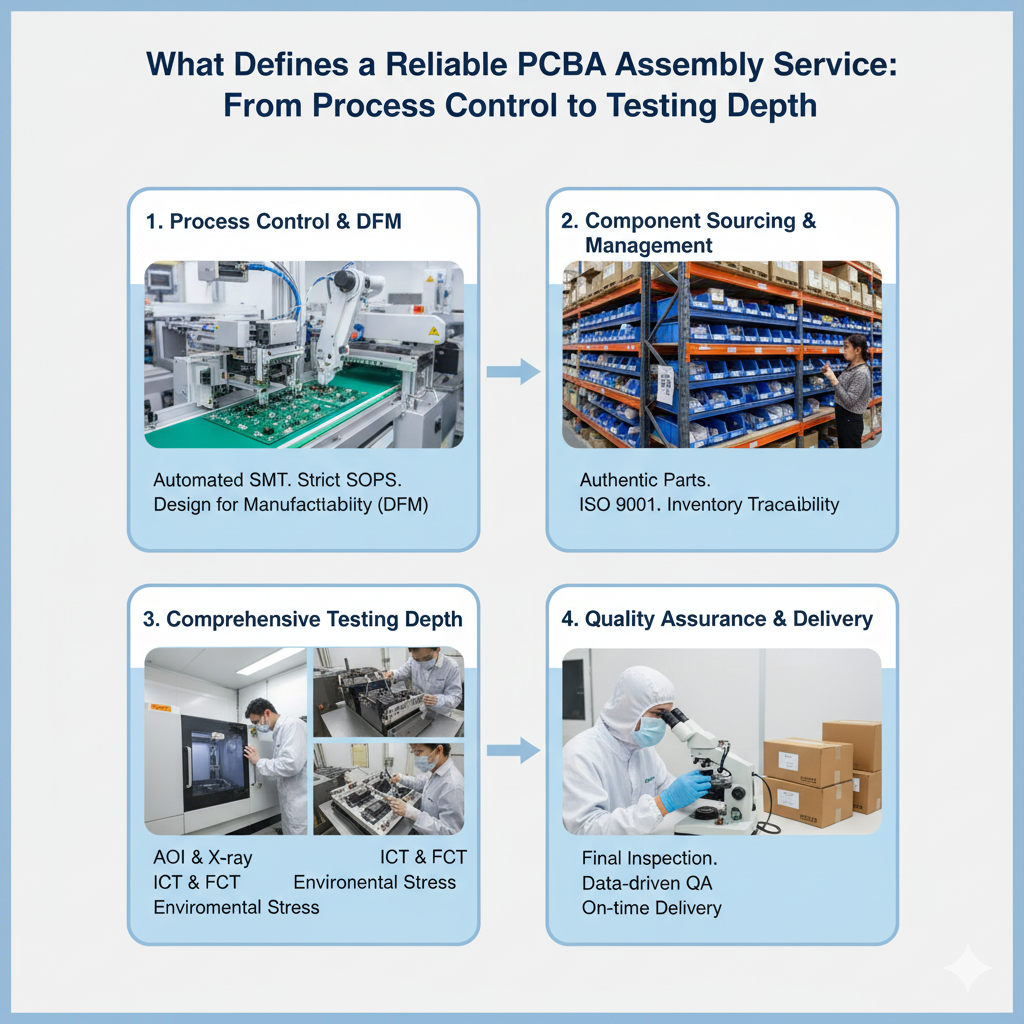
Component Sourcing: Where Cost and Reliability Begin
Every project starts with components, and every failed batch starts with poor sourcing.
A mature electronics manufacturing partner integrates component procurement into its production system to prevent common pitfalls—counterfeit parts, EOL (end-of-life) components, and mismatched packaging.
They evaluate supplier traceability, reel labeling, and moisture sensitivity levels (MSL) before a single reel hits the line.
Proper component sourcing service ensures that every resistor, IC, and connector has the right storage condition, bake cycle, and lot certification.
That’s how cost optimization becomes risk reduction, not cost cutting.
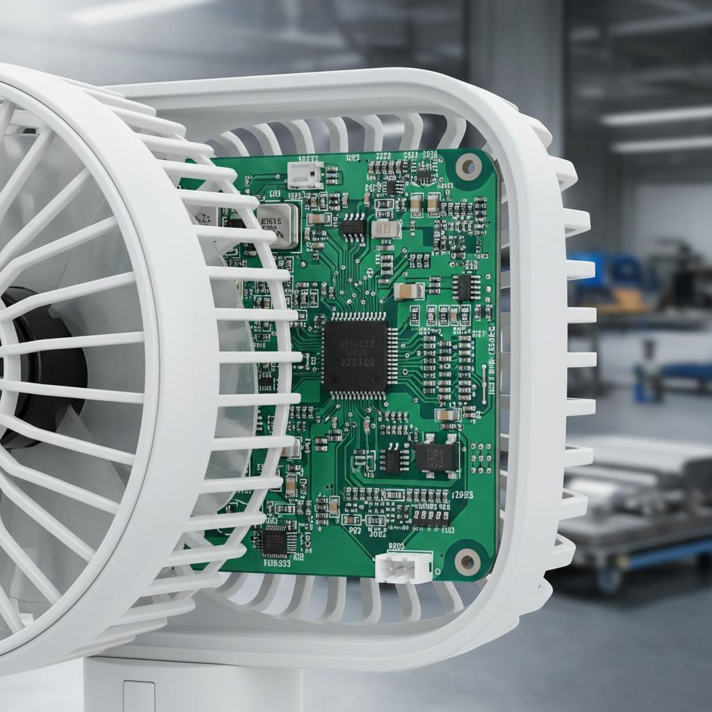
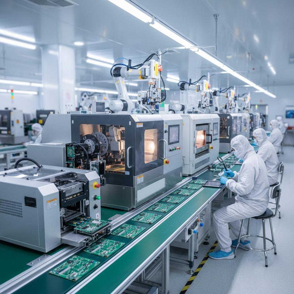
Process Control in Surface Mount Technology (SMT)
Surface mount technology is a field of tight margins—temperature windows measured in degrees, placement precision in microns, and yield differences in fractions of a percent.
Factories with strong turnkey PCB assembly capability implement real-time monitoring for solder paste printing, pick-and-place calibration, and reflow temperature profiling.
| Control Parameter | Engineering Purpose |
|---|---|
| Solder Paste Thickness (±10%) | Maintains uniform wetting and reduces bridging or cold joints. |
| Placement Accuracy (<30 µm) | Ensures fine-pitch ICs and BGAs survive thermal cycling. |
| Reflow Peak Temperature | Balances IMC growth to avoid brittle joints or incomplete fusion. |
| AOI Feedback Loop | Provides process correction after each panel, improving next-run accuracy. |
| Humidity & ESD Monitoring | Prevents latent electrostatic and moisture damage. |
Consistency here isn’t automation—it’s control.
An experienced operator still defines when machines deliver quality.
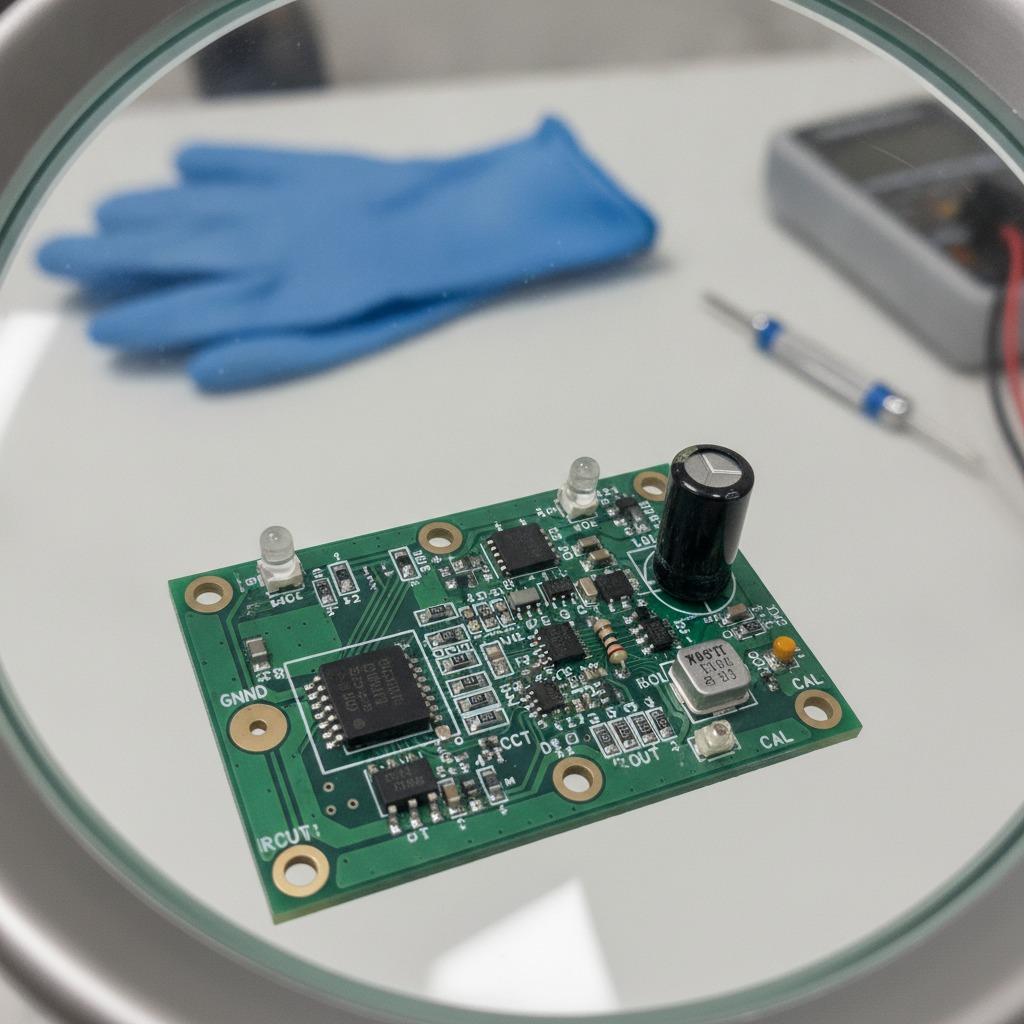
Inspection and Testing: Turning Process Into Proof
No matter how refined the process, verification is the ultimate equalizer.
In professional PCBA assembly services, testing isn’t optional; it’s systemic.
Factories perform sequential inspection at multiple stages to ensure full traceability:
-
SPI (Solder Paste Inspection): Verifies print thickness before placement.
-
AOI (Automated Optical Inspection): Detects misalignment, bridging, and insufficient solder.
-
ICT (In-Circuit Test): Checks continuity, shorts, and impedance at key nodes.
-
FCT (Functional Circuit Test): Simulates real operating conditions to confirm logic stability.
-
Burn-in Testing: Exposes early-life defects through thermal stress.
These checkpoints convert manufacturing confidence into measurable data—exactly what OEMs expect before mass production.
How to Select the Right PCBA Service Based on Project Requirements
Not all PCBA factories suit every type of project. The right choice depends on your design complexity, production scale, and testing requirements.
Here’s how to align your selection with your real needs:
| Project Type | Recommended Factory Capability |
|---|---|
| Prototype / Small Batch | Fast-turn prototyping lines with flexible tooling and on-site engineering support. |
| Consumer Electronics Mass Production | High-speed SMT lines, multi-line scheduling, and full automated AOI/FCT coverage. |
| Industrial / Automotive PCBA | IPC-A-610 Class 3 compliance, environmental testing, and traceable quality management. |
| IoT / Smart Devices | Strong DFM (Design for Manufacturability) collaboration and fine-pitch BGA process capability. |
| Custom OEM Modules | Integrated component sourcing, firmware burning, and complete box-build service. |
When evaluating a vendor, don’t ask only about price.
Ask about process capability, testing transparency, and engineering feedback speed—these determine whether your product will scale successfully, not just pass inspection.
A Partner for Precision and Predictability
The strength of a true PCBA assembly service lies in predictability—turning hundreds of variables into one repeatable outcome: stable performance.
From sourcing to reflow and final inspection, every control loop builds trust into the board.
If you want to explore how our production systems ensure yield consistency and testing coverage for your next project, visit our official website or contact our engineering team via the contact page.
Let’s make reliability measurable, not assumed.