Mastering High Speed Differential Routing PCB for Cutting-Edge Electronics
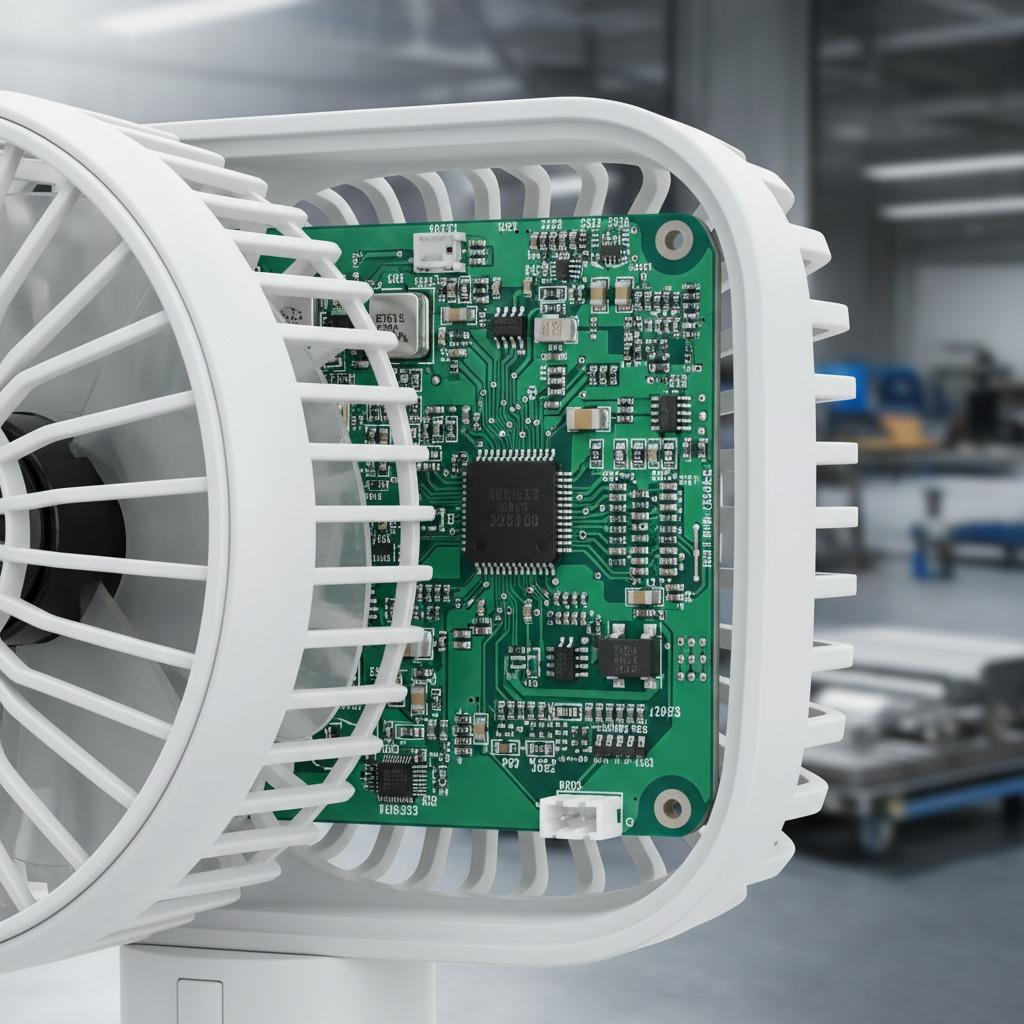
In the fast-paced world of modern electronics, high speed differential routing PCB stands as a cornerstone for achieving reliable, high-performance connections. This technique involves carefully designing paired signal paths on printed circuit boards to transmit data at blazing speeds while minimizing noise and crosstalk. At hcdpcba, we specialize in crafting these intricate boards, leveraging our expertise in multi-layer and high-frequency PCBs to bring your innovative projects to life. Imagine pathways that pulse with precision, carrying signals across vast distances within a compact module, ensuring seamless communication in devices from telecommunications to automotive systems. Our commitment to quality ensures that every high speed differential routing PCB we produce not only meets but exceeds industry standards, fostering durability and efficiency in demanding applications.
Unlocking the Advantages of High Speed Differential Routing PCB
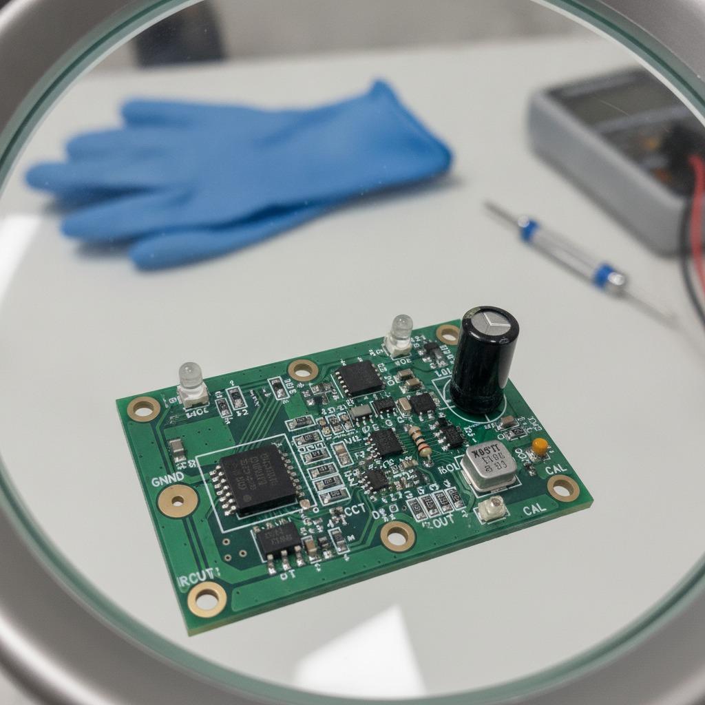
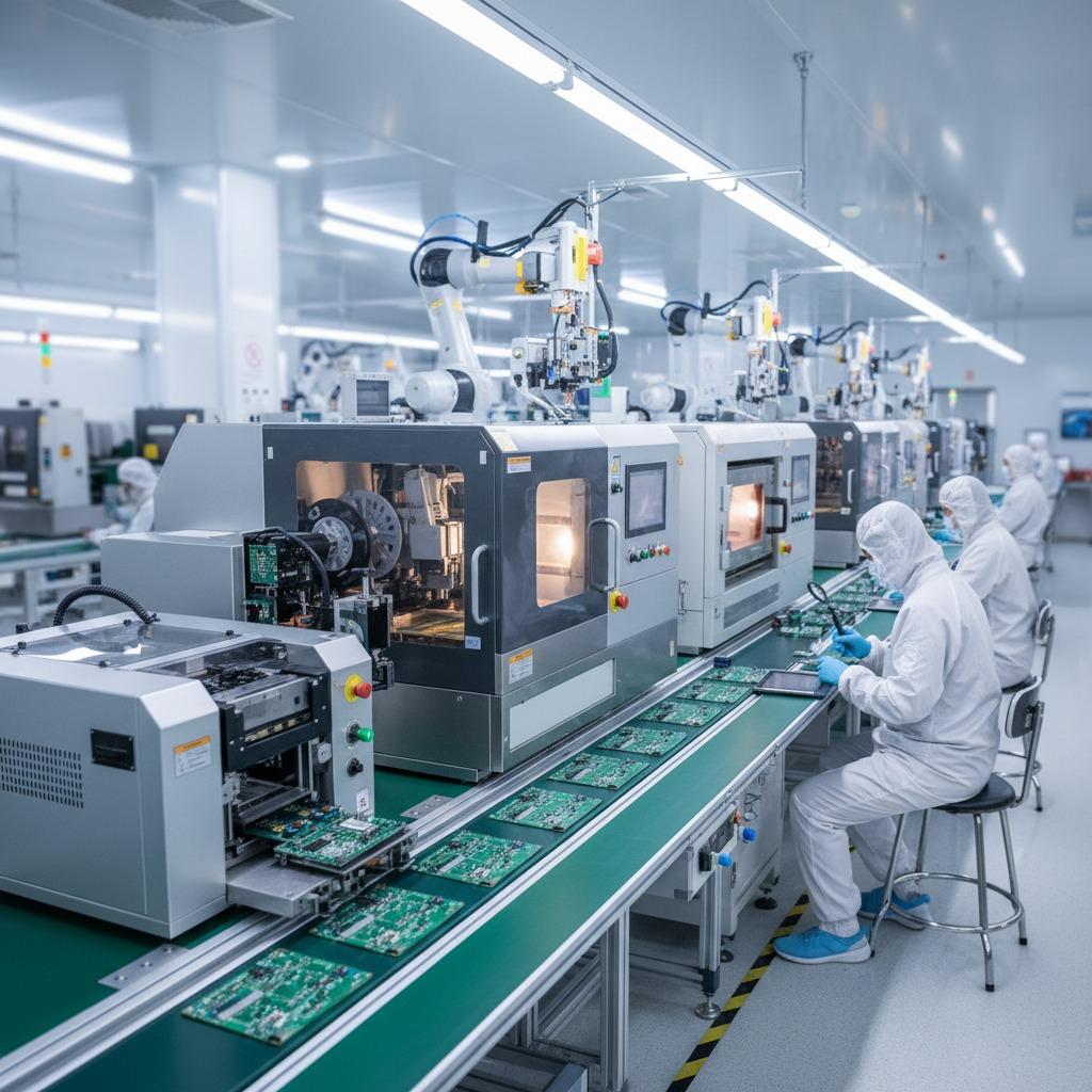
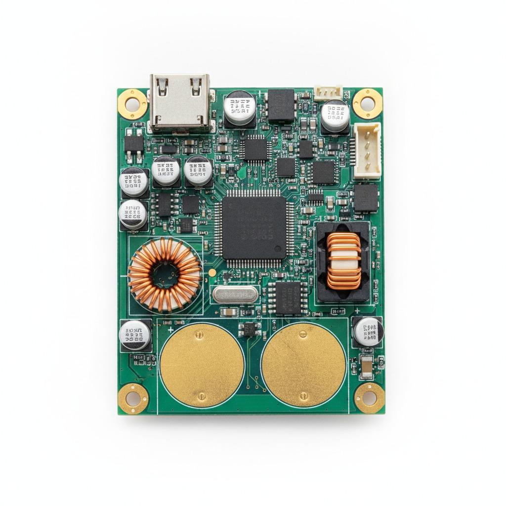
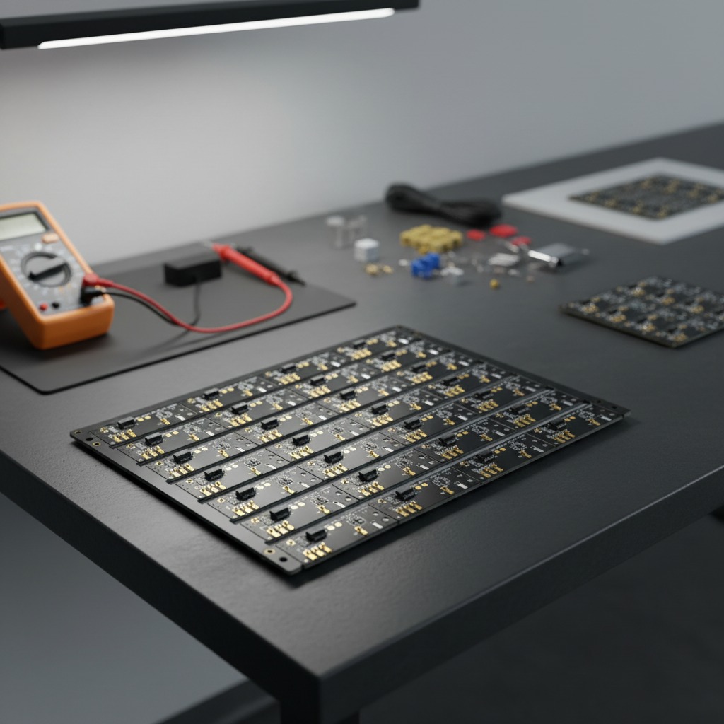
Delve deeper into the artistry of high speed differential routing PCB, where balanced pairs of traces act like vigilant guardians against electromagnetic interference. These routes, meticulously spaced and impedance-matched, allow data to flow at gigabit speeds without degradation, painting a picture of electronic harmony. At hcdpcba, our advanced manufacturing processes, including precision SMT placement and rigorous testing, transform complex designs into tangible realities. Picture a board where golden contacts gleam under light, ready to integrate into optical systems or control units, their robust construction shielding against environmental stresses. This approach not only enhances signal integrity but also reduces power consumption, making it ideal for energy-sensitive applications in IoT and smart homes. Our team's technical prowess ensures that each board is a masterpiece of engineering, optimized for longevity and peak performance.
Seamless Integration with Optical Transceiver PCB Assembly
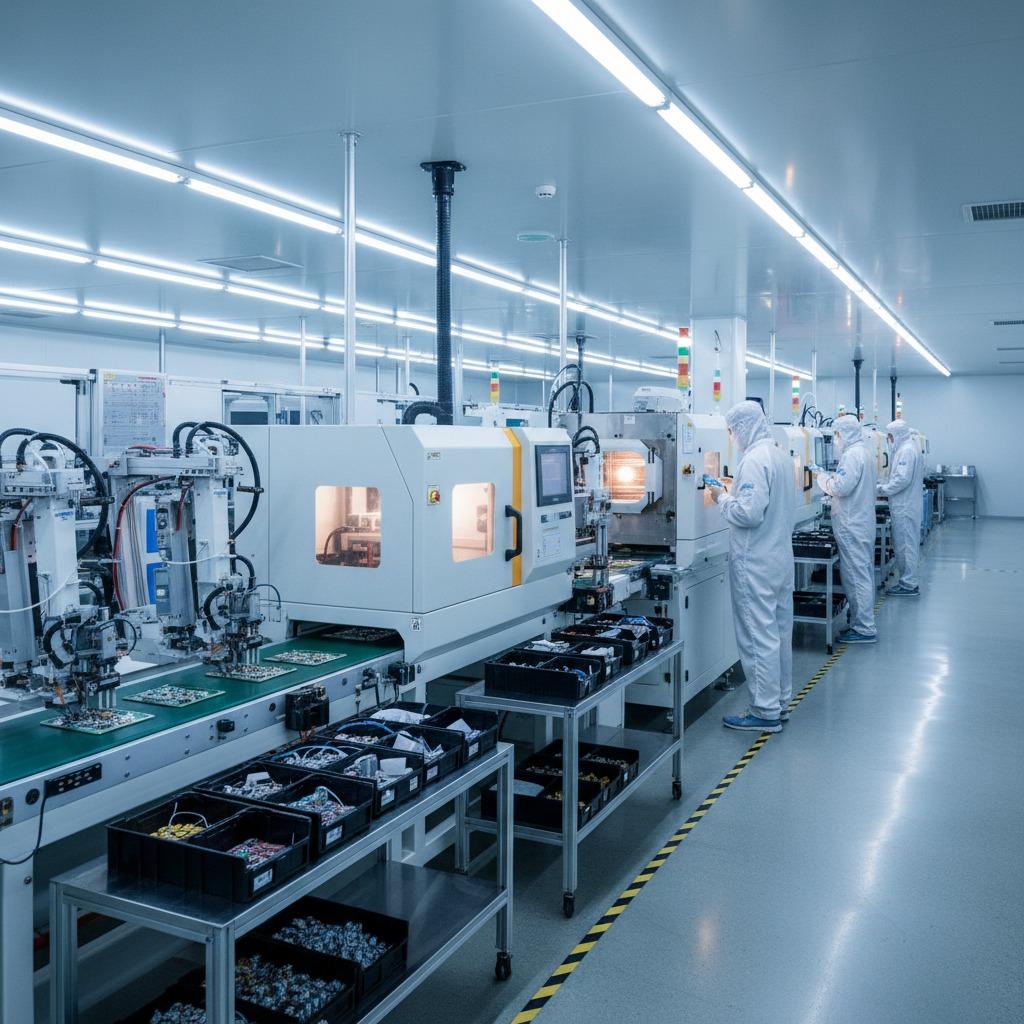
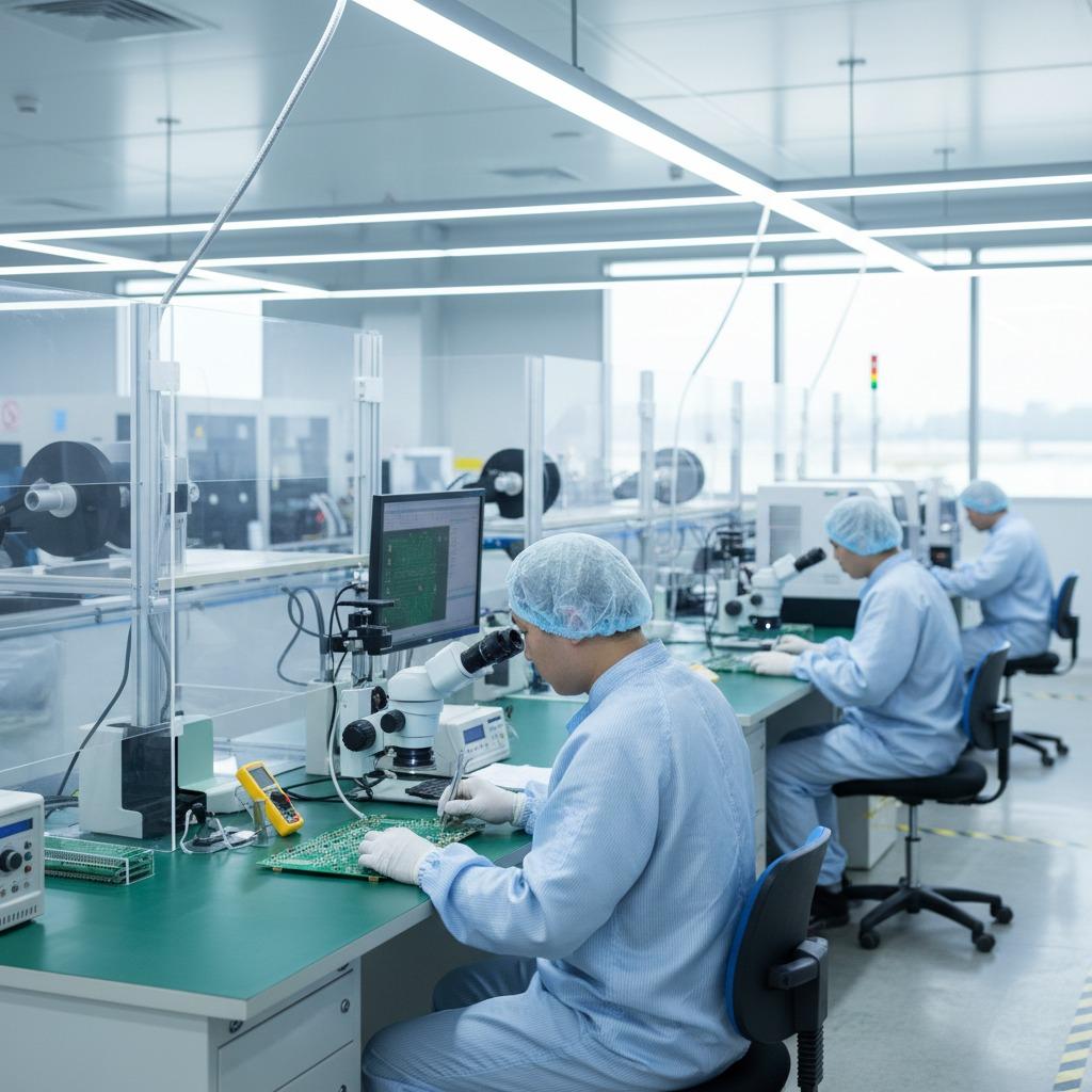
When high speed differential routing PCB meets optical transceiver PCB assembly, the result is a symphony of light and electricity, propelling data transmission into the future. Optical transceiver PCB assembly involves assembling components that convert electrical signals into optical ones, crucial for high-bandwidth networks. At hcdpcba, we offer comprehensive services from PCB prototyping to full assembly, ensuring that optical transceiver PCB assembly aligns perfectly with differential routing needs. Envision compact modules where fiber optics dance alongside precisely routed traces, enabling ultra-fast data transfer in communications and AI-driven devices. Our OEM and ODM capabilities allow for customized solutions, incorporating surface-mount technology for sleek, interference-free designs. With our efficient procurement of genuine components and DFMA analysis, we minimize costs while maximizing reliability, serving industries like medical and automotive with unparalleled precision.
Why Choose hcdpcba for Your High Speed Differential Routing Needs
At hcdpcba, we don't just build boards; we engineer solutions that illuminate possibilities. Our high speed differential routing PCB services are backed by a responsive team ready to handle urgent quotes and productions, all while upholding strict quality controls for zero-defect outcomes. From small-batch SMT pasting to large-scale PCBA for high-frequency applications, our streamlined processes ensure cost-effective, confidential partnerships. Whether you're developing an optical transceiver PCB assembly for telecommunications or a control system for industrial automation, our expertise in multi-layer HDI boards guarantees superior conductivity and signal fidelity. Contact us at +86 18924624188 to explore how we can tailor these technologies to your vision, driving innovation across sectors like security, healthcare, and beyond. With hcdpcba, your projects achieve not just functionality, but excellence in every routed path.