Introduction: Why AI Servers Require High-Density HDI & Multi-Layer PCBA
The rapid iteration of artificial intelligence, big data computing, and cloud data center technology has completely raised the technical threshold for server hardware. Unlike traditional consumer electronic devices, AI servers feature high-load operation, high-frequency signal transmission, and ultra-high component integration. Ordinary standard PCB and common PCBA assembly can no longer adapt to the rigorous requirements of advanced computing hardware in terms of density, heat dissipation, signal stability, and service life.
As a professional OEM/ODM manufacturer focusing on high-end computing circuit solutions, we specialize in high-density HDI PCB assembly and multi-layer advanced computing PCBA tailored exclusively for AI servers, GPU computing modules, data center storage servers, and high-performance industrial computing equipment. We deliver high-precision, high-stability, and high-reliability one-stop PCB & PCBA customization solutions for global AI hardware enterprises.
Core Advantages of HDI PCB Assembly for AI Server Applications
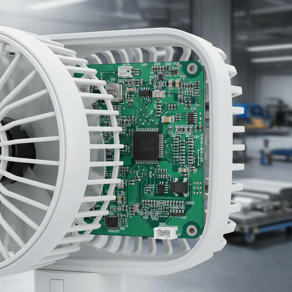
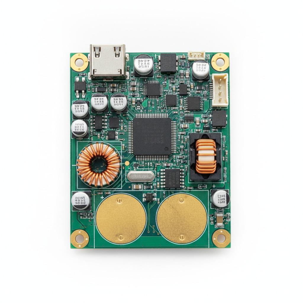
HDI (High Density Interconnect) PCB is the core carrier of modern high-end AI server hardware. Different from conventional circuit boards, HDI boards adopt microvia, laser drilling, buried and blind hole technology, which greatly improves circuit density and wiring accuracy, perfectly matching the miniaturization and high integration trend of AI servers.
1. Ultra-high wiring density, adapting to multi-GPU integrated design
AI servers are usually equipped with multiple high-performance GPUs, TPUs and AI acceleration chips, requiring a huge number of circuit connections in a limited board space. Our HDI PCB assembly adopts advanced sequential lamination and fine-line processing technology, which realizes ultra-fine line width and micro-hole interconnection, effectively increases board utilization, and supports highly integrated layout of core computing chips, memory modules and power modules.
2. Optimized signal transmission, eliminating high-speed computing interference
Long-term high-speed AI model training and data calculation put forward extremely strict requirements on signal integrity. Traditional PCBs are prone to signal loss, crosstalk and delay under 5G+ high-frequency operation. Our HDI PCBA is optimized in stackup design and material selection, which effectively reduces high-frequency signal attenuation, ensures stable transmission of 112Gbps high-speed signals, and guarantees zero-error operation of AI server hardware under long-term full-load working conditions.
3. Lightweight & compact structure, optimizing server space
Data center servers pursue high space utilization and low energy consumption. High-density HDI structure replaces the traditional multi-board splicing design with a single high-integration board, which greatly reduces the overall size and weight of the server motherboard, helps customers optimize equipment structure design, and reduces data center operation and maintenance costs.
Multi-Layer Advanced Computing PCBA: The Core Guarantee of AI Server Stability
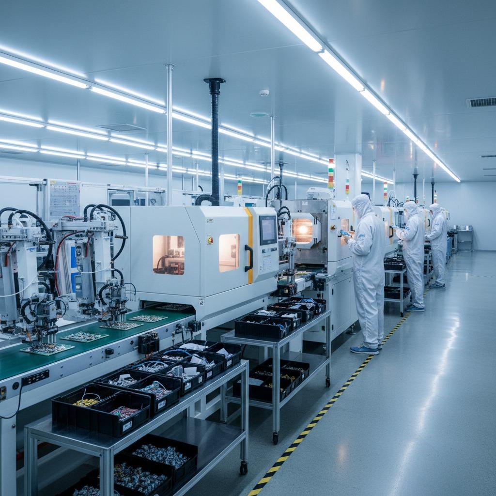
Advanced computing scenarios represented by AI servers, cloud computing and edge computing rely heavily on high-layer high-precision PCBA finished boards. We support 16–32 layer high-layer-count PCB customized production and full-process SMT assembly, focusing on high-end computing hardware circuit manufacturing.
In terms of material selection, we exclusively adopt low-loss high-frequency substrates suitable for advanced computing scenarios, which have excellent heat resistance and dielectric stability. Aiming at the high heat generation problem of AI servers during long-term high-load operation, we adopt professional thermal design and solder joint reinforcement technology in the PCBA assembly process to avoid solder joint aging and circuit failure caused by long-term high-temperature operation.
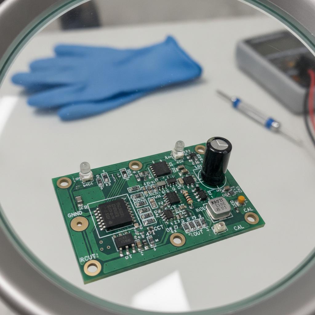
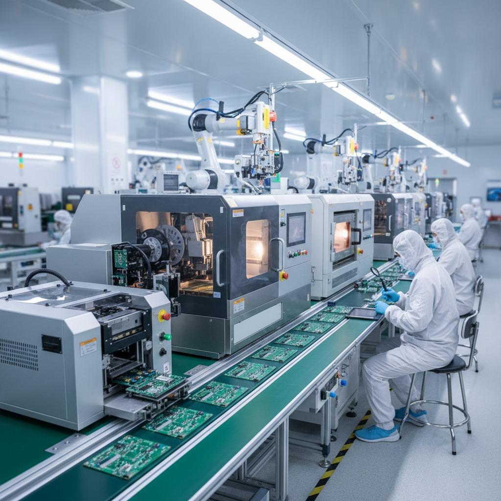
At the same time, we implement full-process quality control for multi-layer PCBA production, including IQC incoming material inspection, IPQC process monitoring, and FQC finished product testing. All finished boards pass strict high and low temperature aging tests, signal integrity tests and functional reliability tests, which can fully adapt to 7*24-hour uninterrupted stable operation of data center AI servers.
Professional OEM/ODM One-Stop PCBA Manufacturing Service
We are not only a PCB production and assembly factory, but also a professional advanced computing circuit solution provider. For global AI hardware startups and medium and large-sized enterprises, we provide flexible and full-link OEM/ODM customized services:
-
Professional PCB stackup design, circuit optimization and scheme customization
-
HDI board, high-layer multi-layer PCB proofing, small batch trial production and mass production
-
High-precision SMT patch, plug-in assembly and soldering processing
-
Functional testing, aging testing and reliability verification
-
Post-production technical adjustment and after-sales support
Whether it is prototype research and development of new AI server products or large-scale mass production of mature equipment, we can adjust production schemes and delivery cycles according to customer needs, greatly saving customers' R&D costs and production cycles.
Why Choose Us for AI Server HDI & Multi-Layer PCBA?
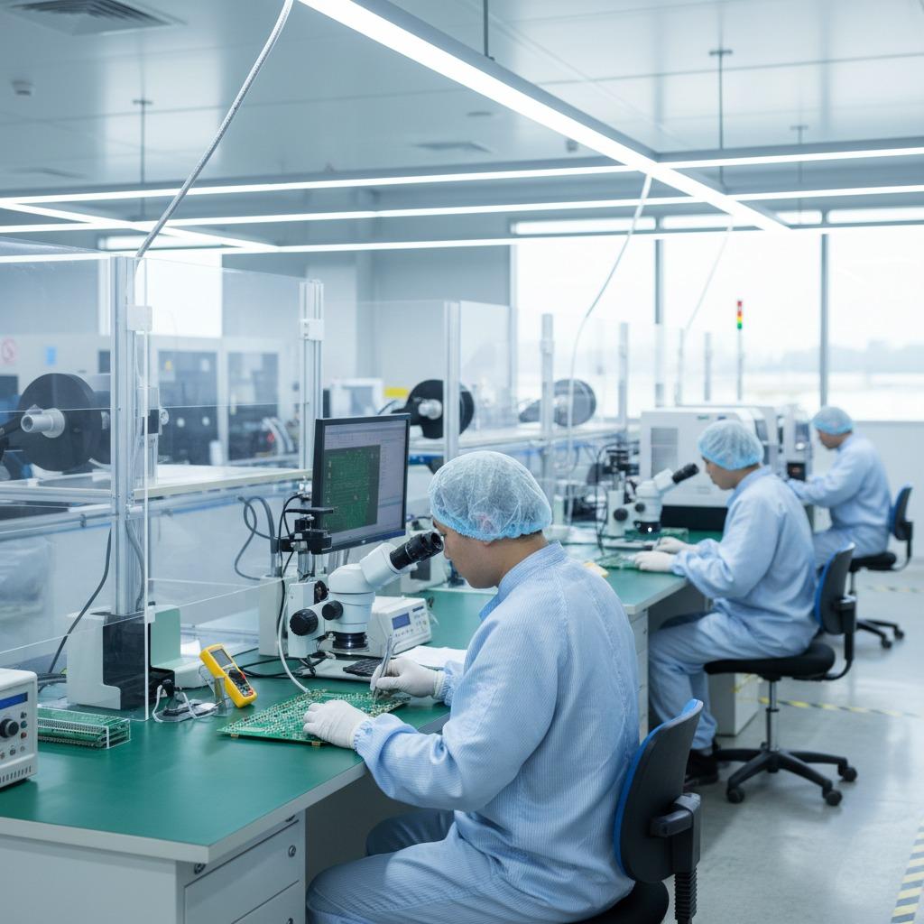
With years of deep cultivation in the field of high-end computing PCB/PCBA, we have accumulated rich project experience in AI servers, high-performance computing, data center equipment and industrial control hardware. We abandon low-end low-density circuit board production and focus entirely on high-precision, high-density, high-reliability advanced computing circuit products.
Equipped with automated production equipment and a professional technical R&D team, we strictly follow international industrial standards in every production link from board manufacturing, patch assembly to finished product testing. We always take high precision, high stability and high customization as the core standard to meet the stringent quality requirements of high-end AI hardware equipment.
Conclusion
With the continuous upgrading of AI computing technology, high-density HDI PCB and multi-layer high-speed PCBA will become the standard configuration of mainstream AI server hardware. Choosing high-quality advanced computing circuit board manufacturers is the key to ensuring product competitiveness and equipment stability.
If you are looking for a reliable AI server HDI PCB assembly and multi-layer PCBA OEM/ODM manufacturer, welcome to contact us for free technical solution consultation, product quotation and sample testing support. We look forward to creating high-value advanced computing hardware solutions with you.