HD Camera Module Manufacturer: Building High-Definition Vision with Precision and Stability
Every sharp, detailed image starts with engineering excellence you cannot see.
From the alignment of microscopic pixels to the synchronization of optical lenses and signal processors, a professional HD camera module manufacturer transforms electronic precision into visual clarity.
Whether used in smartphones, surveillance, automotive vision, or industrial inspection, these modules are the bridge between light and logic—where every micron matters.
Core Structure of an HD Camera Module
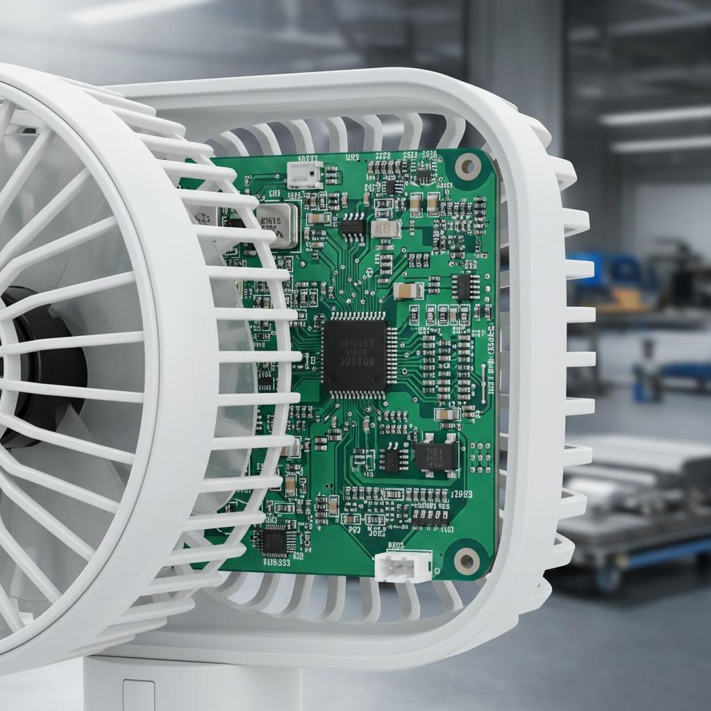
An HD camera module is more than a combination of lenses and sensors; it’s a tightly integrated electro-optical system.
| Component | Function | Manufacturing Focus |
|---|---|---|
| CMOS Image Sensor | Captures light and converts it to data | Pixel alignment, noise suppression |
| Lens Assembly | Focuses and directs light accurately | Axis alignment ≤3μm, distortion correction |
| ISP (Image Signal Processor) | Processes brightness, color, and focus | Controlled impedance on PCBA |
| Driver and Connector Board | Provides power and communication | Solder joint reliability, trace routing |
| Protective Housing | Ensures mechanical integrity | Dust-free sealing and vibration resistance |
Each component interacts seamlessly to convert photons into precise electrical signals—forming the foundation of HD imaging systems.
Precision in Sensor and Lens Alignment
High-resolution imaging depends on sub-micron alignment accuracy between the lens and CMOS sensor.
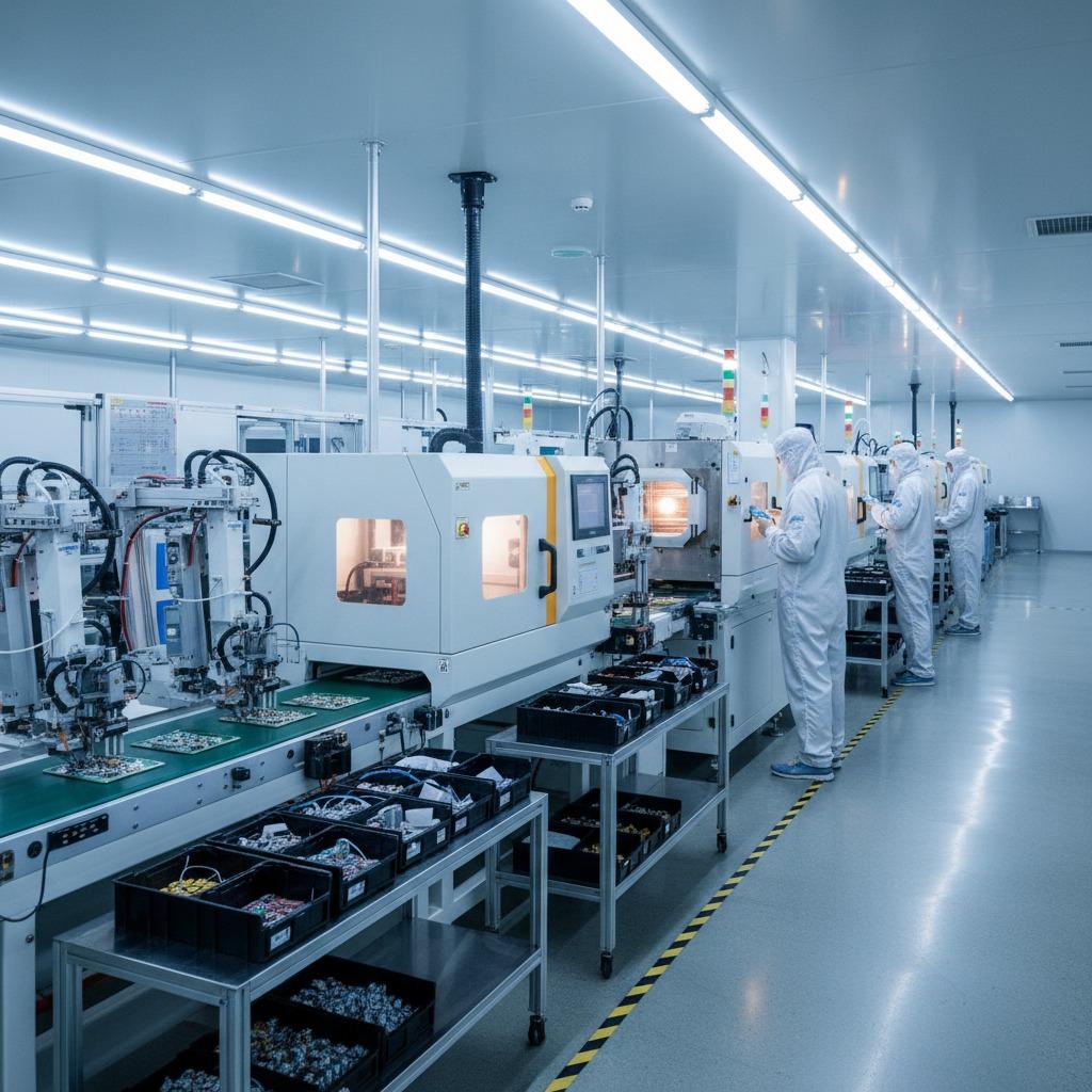
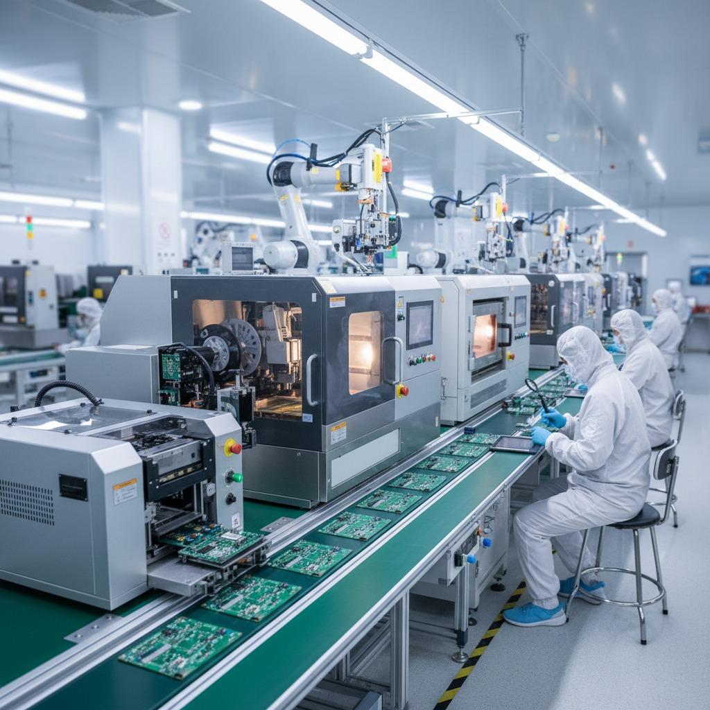
To achieve this, HD camera module factories implement advanced automated systems and optical calibration technologies:
-
Active alignment equipment that adjusts position in six axes during real-time optical feedback.
-
Laser measurement systems that ensure focus uniformity across all corners.
-
Cleanroom assembly (Class 100–1000) to eliminate dust-induced optical artifacts.
-
Temperature-controlled bonding stations to minimize stress and lens warping.
-
Vision-guided robotic placement for reproducible optical centering.
This ensures perfect image uniformity, color accuracy, and depth fidelity—critical for HD and 4K applications.
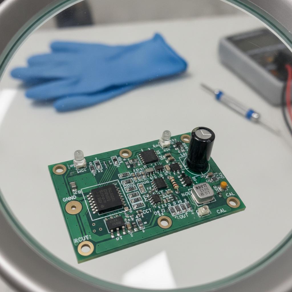
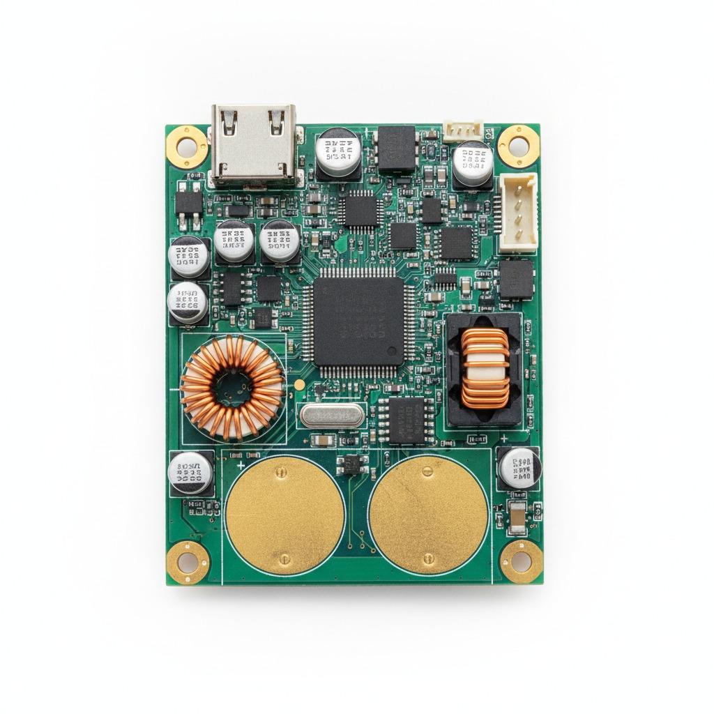
High-Performance PCBA Integration for Image Stability
An HD camera module’s performance depends not only on optics but also on its electronics.
The embedded image signal processor (ISP) and driver PCBA regulate exposure, manage noise, and ensure real-time color balance.
Key electronic design and assembly highlights include:
-
4-layer PCB architecture for stable signal routing and EMI shielding.
-
Differential impedance control for MIPI/LVDS high-speed data lines.
-
Low-ripple power management circuits for CMOS sensor protection.
-
Thermal dissipation structures that stabilize performance under continuous operation.
-
Firmware calibration to optimize color matrix, gain, and white balance per module batch.
Through these steps, every board ensures consistent image quality—even in demanding lighting or environmental conditions.
Optical Module Calibration and Color Optimization
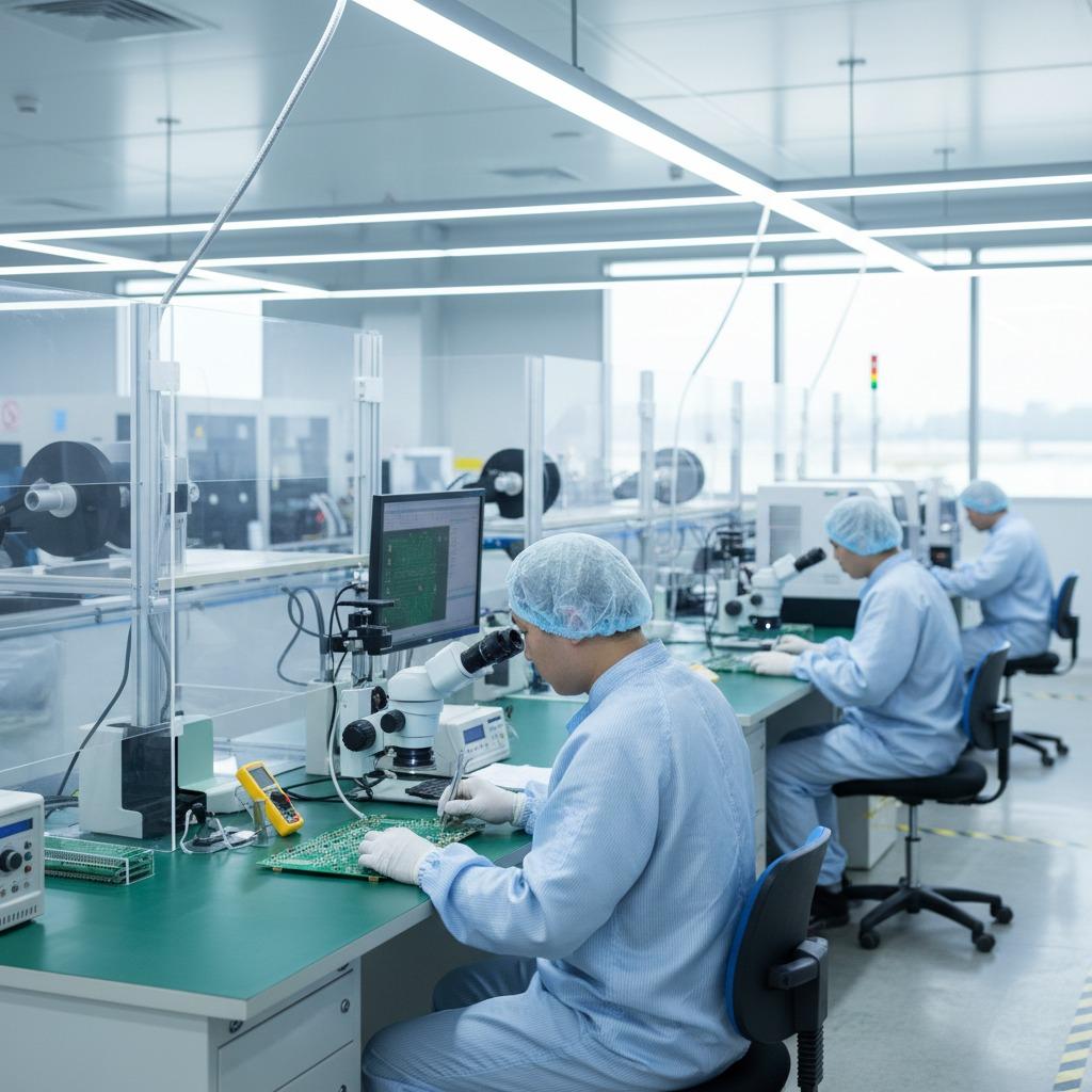
Manufacturing an HD camera module extends beyond assembly—it requires optical fine-tuning.
Factories conduct multiple calibration stages to guarantee brightness uniformity, focus consistency, and accurate color reproduction.
| Calibration Step | Objective | Tools and Technology |
|---|---|---|
| Focus Calibration | Define sharpness range and auto-focus accuracy | Laser interferometry systems |
| White Balance Adjustment | Correct color deviation | Spectral light sources & software tuning |
| Field Uniformity Test | Ensure even brightness | AI-assisted image analysis |
| Chromatic Aberration Correction | Remove edge distortion | Multi-spectral simulation |
| Optical Center Validation | Verify alignment accuracy | CCD-based optical inspection |
These processes guarantee that HD camera modules perform consistently across production batches and environmental variations.
Reliability and Environmental Testing
High-definition performance means little without long-term stability.
To ensure reliability, every HD camera module undergoes rigorous validation before mass production.
| Test Type | Purpose | Conditions |
|---|---|---|
| Thermal Cycling Test | Validate performance under temperature swings | -40°C to +85°C |
| Vibration & Drop Test | Confirm structural integrity | 3-axis, 50Hz–500Hz |
| Humidity Resistance | Prevent lens fogging and corrosion | 60°C, 90% RH |
| Aging Test | Simulate continuous use | 72-hour burn-in |
| Optical Clarity Test | Detect focus and color anomalies | Real-time visual inspection |
Only after passing these tests can a module meet the rigorous standards demanded by HD imaging applications in consumer and industrial markets.
Advantages of Choosing a Professional HD Camera Module Manufacturer
Partnering with a specialized HD camera module manufacturer ensures not just product quality—but consistent innovation and supply reliability.
Key advantages include:
-
Integrated Optical-Electronic Manufacturing – From PCBA to lens calibration, all in-house.
-
Cleanroom Assembly and Quality Control – Ensures contamination-free optical precision.
-
High-Speed Automated Alignment – Enhances accuracy and throughput.
-
Industry-Grade Reliability Standards – ISO-certified, RoHS-compliant production.
-
Customized Module Design – Tailored solutions for automotive, security, and industrial imaging.
Such expertise enables faster prototyping, scalable production, and superior imaging stability for OEM partners worldwide.
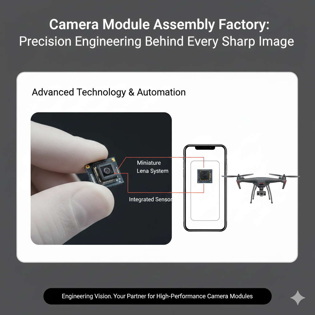
Applications Across Industries
HD camera modules power a wide range of modern imaging applications:
-
Smartphones and tablets for ultra-clear photo and video capture.
-
Automotive ADAS systems for lane detection and parking assist.
-
Industrial inspection systems requiring precise visual detection.
-
Smart home devices for real-time monitoring and AI analytics.
-
Medical imaging tools where color accuracy and depth detail are critical.
From consumer electronics to industrial automation, HD modules redefine what “clarity” means in digital vision.
Delivering Clarity at Every Pixel
Every pixel of an HD image is built on precision engineering.
A reliable HD camera module manufacturer doesn’t just assemble components—it crafts visual performance that endures across millions of frames.
For businesses seeking precision imaging, consistent calibration, and scalable production, explore our professional manufacturing capabilities at www.hcdpcba.com or contact our engineers directly via the contact page.
Because when every pixel matters, precision starts on the factory floor.