Unlocking Excellence in Signal Integrity PCB Design
In the fast-paced world of electronics, achieving flawless signal integrity PCB is paramount for ensuring that data flows without distortion or loss. At hcdpcba, we specialize in crafting PCBs that prioritize signal integrity PCB principles, enabling seamless performance in demanding applications. Our expertise in this area stems from years of dedicated service in PCB design and manufacturing, where we've helped countless clients in telecom, networking, and communication sectors bring their visions to life. Imagine a circuit board where every trace conducts signals with precision, free from the chaos of noise and interference— that's the vivid reality we deliver through our tailored signal integrity PCB solutions.
Mastering Signal Integrity in Telecom PCB Design
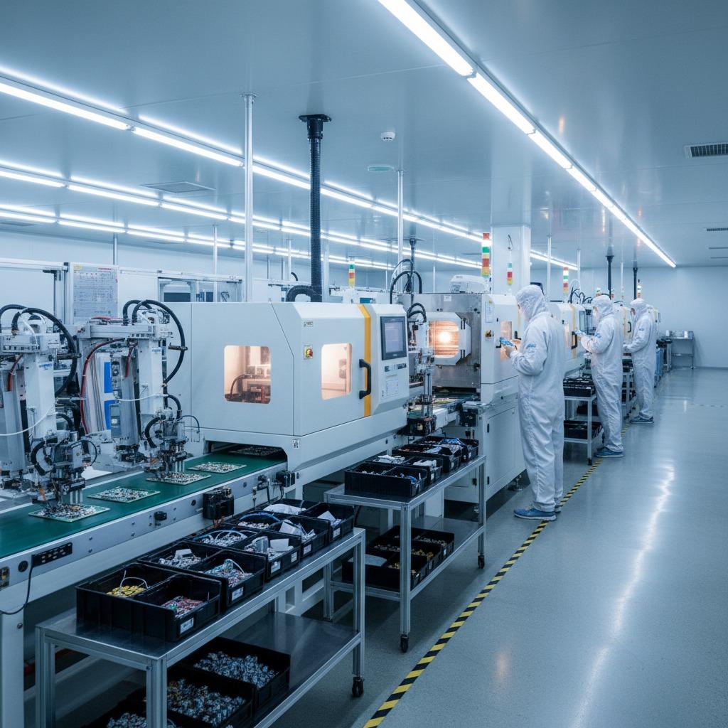
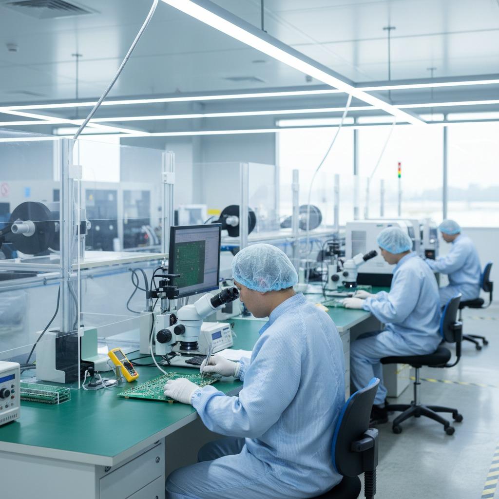
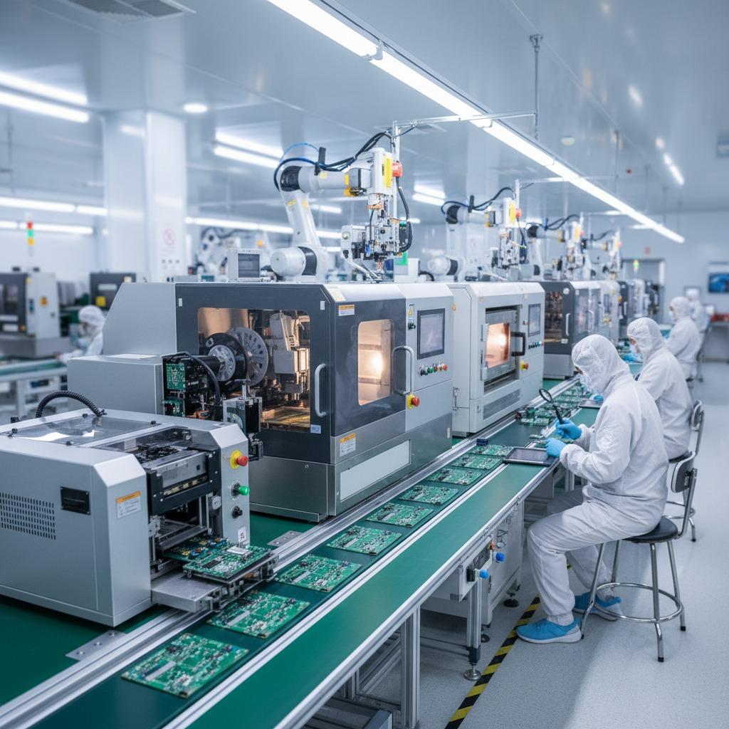
Telecom PCB design demands unwavering reliability, especially when high-frequency signals race through intricate pathways. Our signal integrity PCB approach integrates advanced simulation tools and meticulous layout strategies to mitigate crosstalk and reflections, ensuring your telecom systems operate at peak efficiency. Picture a bustling telecom network where data packets traverse miles without a hitch, powered by our robust telecom PCB design that incorporates impedance matching and controlled dielectric materials. At hcdpcba, we offer comprehensive telecom PCB design services, including SMT pasting and PCBA assembly, all backed by our experienced team. This not only enhances signal integrity PCB but also aligns with our commitment to quality assurance, where every board undergoes rigorous testing to guarantee zero defects. Clients in the communications industry rave about how our telecom PCB design has transformed their products, making them faster and more dependable in real-world deployments.
Enhancing Reliability with Network Interface PCB
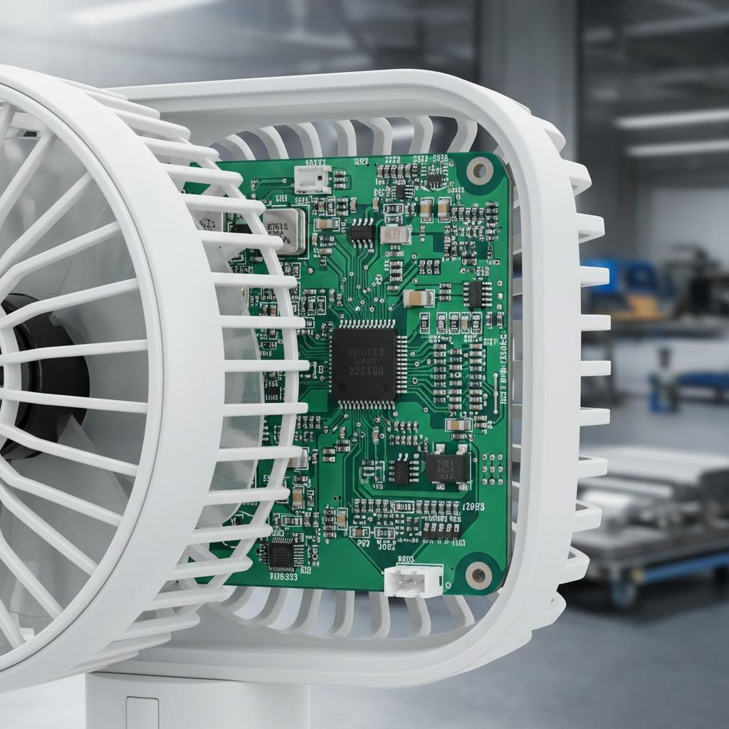
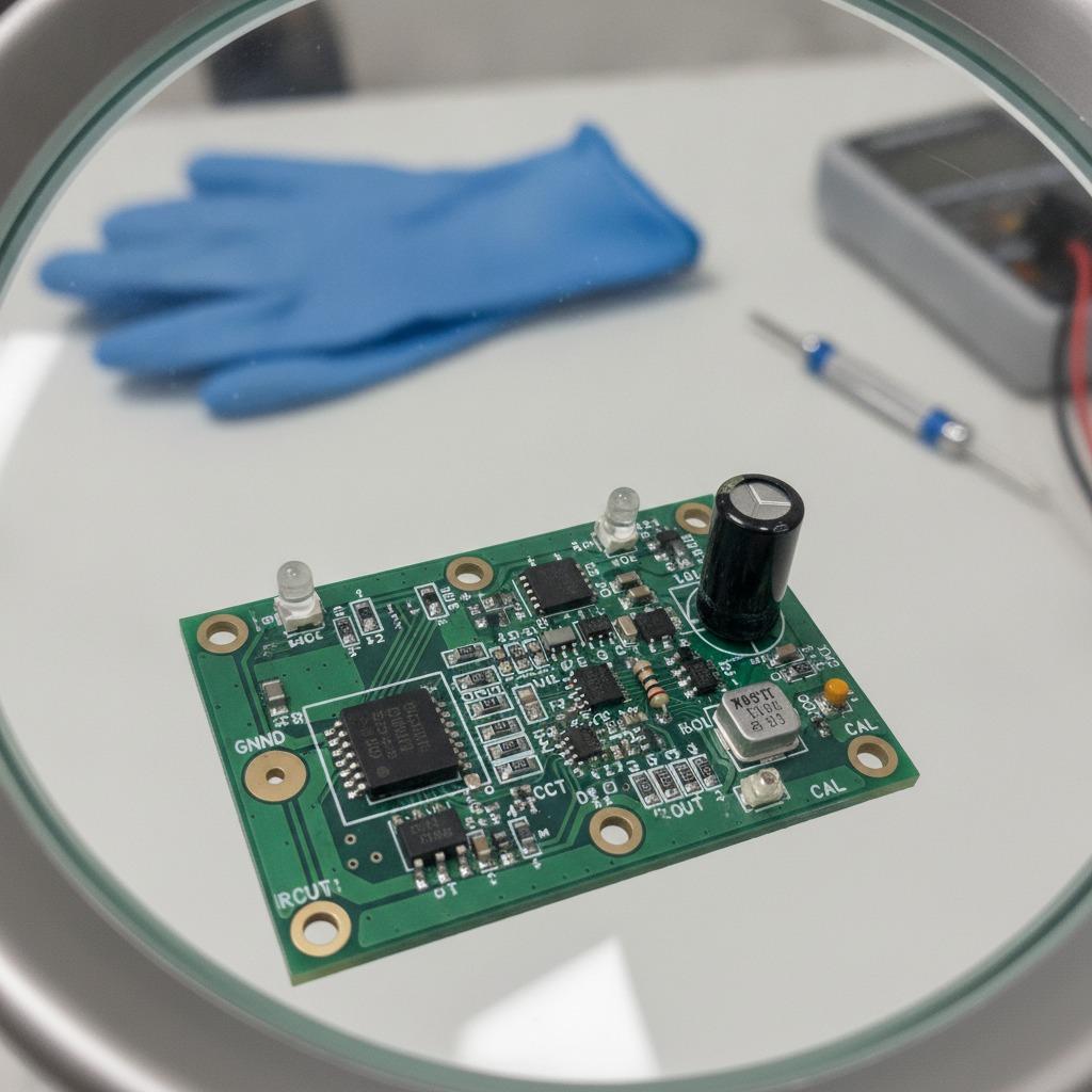
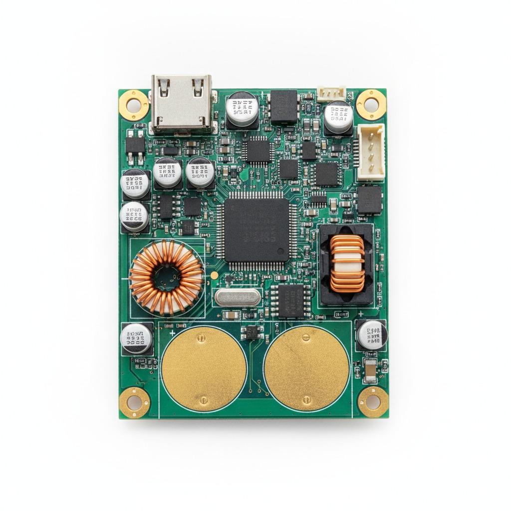
When it comes to network interface PCB, signal integrity PCB becomes the backbone of uninterrupted connectivity. Our designs feature optimized routing and shielding techniques that preserve signal quality even under heavy loads, vividly illustrating a network hub that hums with consistent data throughput. Integrating elements like our ANX7438 development board, which boasts a powerful chipset and integrated Ethernet port, we ensure network interface PCB solutions that support high-speed transfers ideal for IoT and robotics. hcdpcba's network interface PCB services extend to DFMA analysis, helping reduce costs while maintaining superior signal integrity PCB standards. Envision sensors and peripherals linking effortlessly, their signals clear and strong, thanks to our plug-and-play connectors and thorough component procurement. This holistic approach not only boosts performance but also fortifies your systems against environmental rigors, a testament to our sturdy, versatile builds.
Optimizing Communication Chipset PCB for Future-Proof Innovation
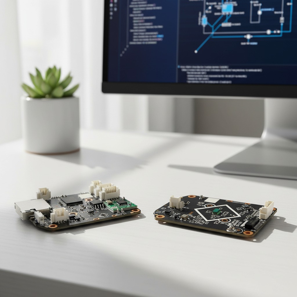
The realm of communication chipset PCB thrives on precision, where signal integrity PCB safeguards against timing skews and attenuation in chipset interactions. At hcdpcba, we vividly craft these boards to handle complex algorithms with ease, incorporating multi-layer HDI and high-frequency materials for telecom PCB design excellence. Our communication chipset PCB solutions, paired with OEM and ODM services, allow for customized innovations that integrate seamlessly with motor systems and AI projects. Think of a compact board pulsing with life, its Ethernet-enabled network interface PCB facilitating rapid data exchange in smart homes or automotive electronics. We limit signal disruptions through advanced testing protocols, ensuring every communication chipset PCB meets stringent industry standards. Our rapid prototyping via PCB打样 services accelerates your development, while cost-effective assembly keeps projects on budget without compromising the vivid reliability that defines our brand.
Why Choose hcdpcba for Your Signal Integrity Needs
Choosing hcdpcba means partnering with a leader in signal integrity PCB, where our telecom PCB design, network interface PCB, and communication chipset PCB expertise converges to deliver unparalleled results. From initial design to final testing, our one-stop services—including元器件代采 and comprehensive quality checks—paint a picture of efficiency and trust. We've empowered industries like medical devices and intelligent power systems with boards that withstand the test of time, all while upholding strict confidentiality. Contact us at +86 18924624188 to explore how our signal integrity PCB innovations can elevate your next project, blending technical prowess with responsive, high-value support.