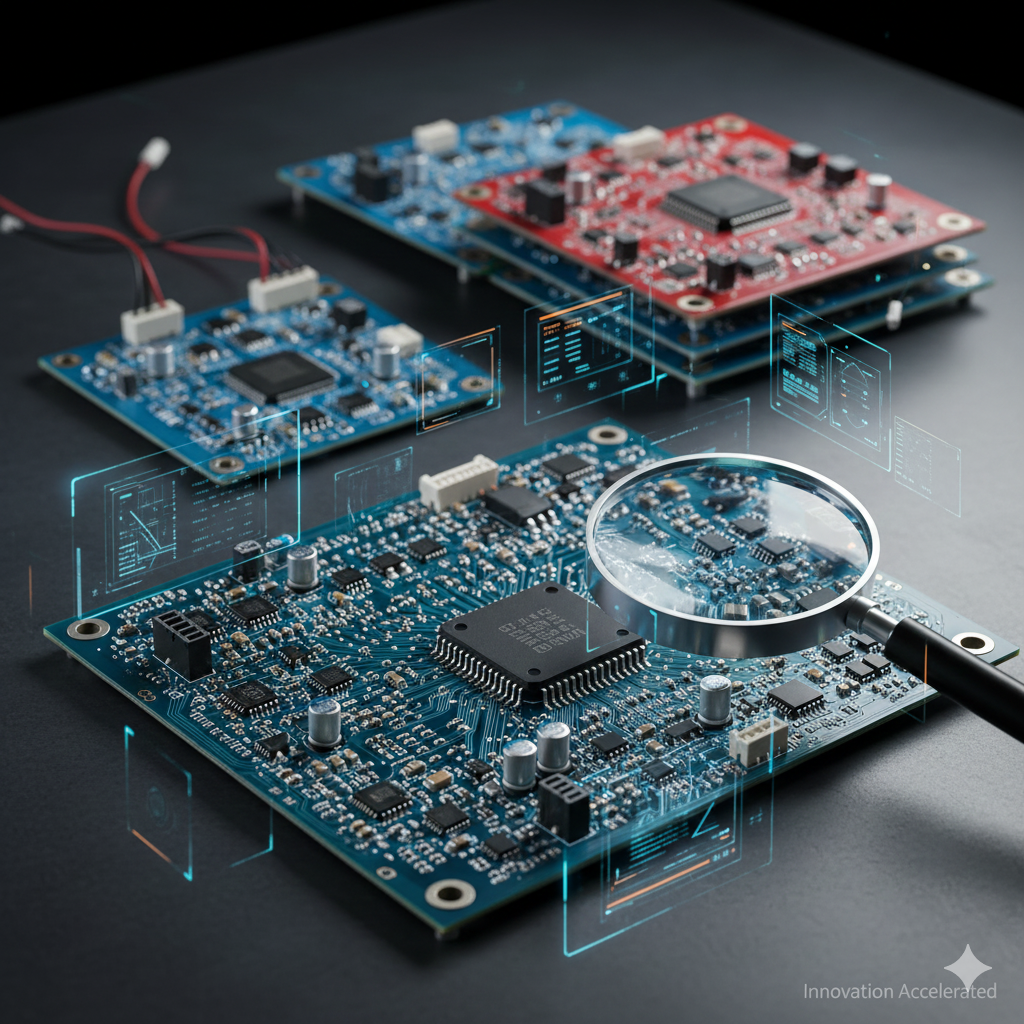
Quick-Turn PCBA Prototype Service: Accelerating Product Validation from Concept to Launch
Innovation doesn’t wait for long lead times.
In a market where new devices enter production every quarter, the ability to move from schematic to working prototype within days defines competitive advantage.
That’s where a quick-turn PCBA prototype service becomes essential—turning design files into tested boards before competitors even start tooling.
This stage isn’t just about speed. It’s about learning faster, validating smarter, and minimizing costly redesigns before full-scale production.
From Design File to Prototype: How the Process Works
In rapid prototyping, time is currency.
Every hour spent waiting on component sourcing or line setup delays market entry.
That’s why modern manufacturers build rapid PCB prototyping systems around digital workflows and parallel operations.
| Stage | Key Action | Turnaround Optimization |
|---|---|---|
| 1. Data Intake | Import Gerber, BOM, and pick-and-place files | Automated DFM check within 2 hours |
| 2. Material Allocation | Verify inventory and alternates | Real-time ERP link for immediate sourcing |
| 3. SMT Setup | Load verified stencil and program placement | Pre-calibrated feeders and stored profiles |
| 4. Assembly | Solder reflow, AOI, and inspection | Single-line processing for 24h builds |
| 5. Testing | ICT/FCT functional validation | Integrated QA stations for instant report |
| 6. Shipment | ESD-safe packing and export labeling | Ready for dispatch within 72 hours |
Each step is synchronized through MES control, enabling small-lot production with prototype turnaround time as short as 48–72 hours.
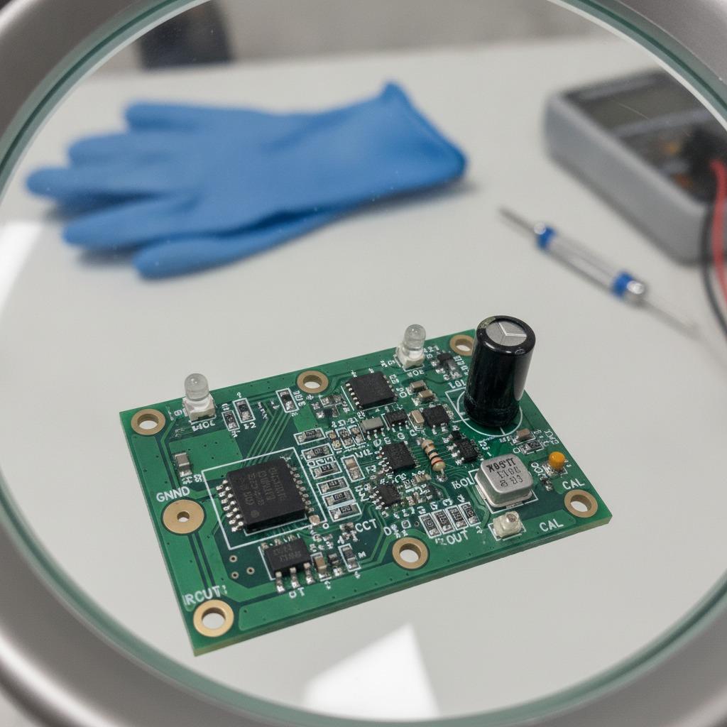
DFM Verification: Reducing Risk Before Volume Production
Speed alone is meaningless without accuracy.
Before scaling up, every design must pass DFM verification—the bridge between engineering intention and manufacturing reality.
In quick-turn PCBA, DFM validation checks for:
-
Pad-to-trace clearance and component spacing violations
-
Solder mask alignment and paste aperture accuracy
-
Thermal relief and copper balancing for even reflow
-
BOM alternates for EOL or long-lead components
-
Mechanical interference between connectors or shields
This analysis prevents costly re-spins and ensures the prototype represents true production behavior—not just a lab sample.
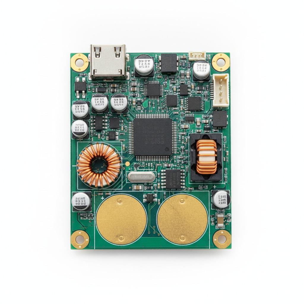
NPI PCBA Builds: The Bridge Between Prototype and Mass Production
A well-executed prototype should transition seamlessly into NPI PCBA builds.
This is where manufacturers integrate both agility and control.
Leading quick-turn suppliers maintain:
-
Dedicated prototype lines separated from high-volume production to avoid scheduling conflicts.
-
Cross-trained teams capable of running multiple builds per day.
-
Component kitting systems that support both customer-supplied and vendor-managed parts.
-
Closed-loop feedback between design and production teams to capture lessons from each iteration.
The result is a consistent handoff from prototype validation to scalable manufacturing, without data loss or requalification.
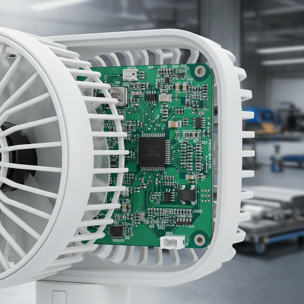
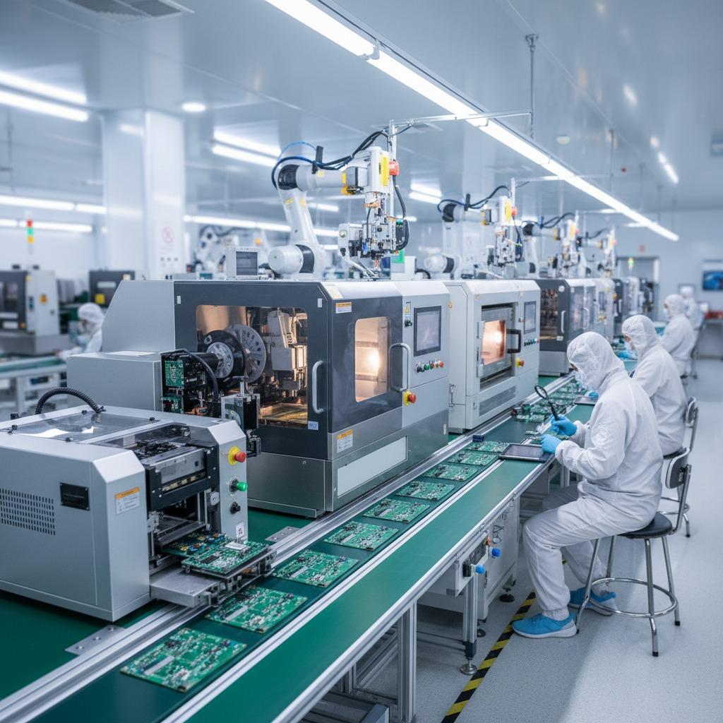
Key Technologies Powering Fast PCB Assembly
Behind every rapid build is a set of technologies that eliminate waiting time.
Modern fast PCB assembly facilities combine precision automation and data-driven process control:
| Technology | Function | Benefit |
|---|---|---|
| High-Speed Pick & Place | 0201–BGA placement with ±25µm accuracy | Handles diverse designs in single shift |
| Reflow Profiling Database | Auto-adjusts heat zones by board type | Prevents cold joints or overheating |
| Inline AOI & SPI | Real-time optical correction | Minimizes defects in micro-assembly |
| Smart Material Tower | Automated reel retrieval | Reduces line setup time by 60% |
| MES Traceability Integration | Records every build parameter | Ensures total production visibility |
With these systems, a single operator can manage multiple prototype orders simultaneously—balancing speed and reliability without compromise.
Delivering Value Beyond Speed
The best quick-turn PCBA prototype service isn’t just a race against time—it’s a strategic asset.
By accelerating iteration cycles and validating manufacturability early, it reduces total project cost and technical risk.
Key customer benefits include:
-
Shorter R&D cycles and faster investor demos
-
Early discovery of design or sourcing bottlenecks
-
Improved transition to NPI and mass production
-
Documented traceability for quality audits
-
Predictable lead times even with design changes
In short, fast doesn’t mean rushed—it means ready.
Turning Ideas into Tested Boards—Fast and Reliable
For developers, startups, and OEMs, time-to-market is the real competitive edge.
A reliable quick-turn PCBA prototype service ensures you can test, refine, and deliver working hardware in record time—without compromising build quality or traceability.
Explore our rapid prototyping capabilities at our homepage.
For direct project consultation or express quotation, connect with our engineers via the contact page.
Every idea deserves a working prototype—and every prototype deserves to be production-ready.