Multilayer PCBA Manufacturer: Supporting High-Density and Signal-Stable Electronics
As electronic products continue to shrink while functionality expands, multilayer PCBAs have become the foundation of modern hardware design. From compact consumer devices to industrial controllers and communication systems, multilayer assemblies enable dense routing, improved signal control, and greater circuit flexibility.
A capable multilayer PCBA manufacturer does far more than stack copper layers. The value lies in how those layers are fabricated, aligned, assembled, and validated to ensure long-term electrical stability and manufacturing consistency.
1. Why Multilayer PCBA Is Essential for Modern Electronics
Single- and double-layer boards are no longer sufficient for products that require complex logic, fast data transmission, and compact form factors. Multilayer PCBAs allow designers to separate signal, power, and ground planes while maintaining tight layouts.
Typical advantages include:
-
Higher routing density without increasing board size
-
Dedicated ground and power planes for noise reduction
-
Shorter signal paths supporting higher data rates
-
Better thermal distribution across layers
-
Improved mechanical stability for larger assemblies
These benefits make multilayer PCBAs a standard choice for advanced electronics rather than a niche solution.
2. Layer Stack-Up Design and Fabrication Control
The performance of a multilayer PCBA begins at the stack-up level. Layer count alone does not determine quality—how each layer is arranged, aligned, and laminated has a direct impact on signal behavior and yield.
A professional manufacturer focuses on:
-
Controlled dielectric thickness between signal layers
-
Accurate layer-to-layer registration
-
Consistent copper weight distribution
-
Reliable via structures (through, blind, or buried vias)
-
Stable lamination cycles to prevent warpage
These factors ensure that the electrical characteristics designed on paper are preserved in real production.
3. Assembly Challenges in High Layer Count PCBAs
As layer count increases, assembly tolerance becomes tighter. Dense routing often leads to smaller pads, finer pitch components, and reduced margin for solder variation.
Multilayer PCBA assembly typically involves:
-
Fine-pitch placement for processors, memory, and RF chips
-
Careful solder paste volume control to avoid bridging
-
Reflow profiles tuned for thicker boards
-
Enhanced AOI coverage for densely populated areas
-
X-ray inspection for hidden solder joints
Without these controls, even a well-designed multilayer board can suffer from reliability issues during operation.
4. Signal Integrity and Power Stability Considerations
Multilayer PCBAs are often used in systems where signal quality is critical—high-speed interfaces, camera data links, power management circuits, and wireless communication modules.
Key manufacturing considerations include:
-
Impedance-controlled routing for high-speed signals
-
Proper ground referencing across layers
-
Isolation between noisy power circuits and sensitive signals
-
Low-inductance power distribution networks
-
Consistent via impedance across the board
A manufacturer experienced with multilayer designs understands how fabrication and assembly decisions directly influence electrical performance.
5. Testing Strategy for Multilayer PCBA Reliability
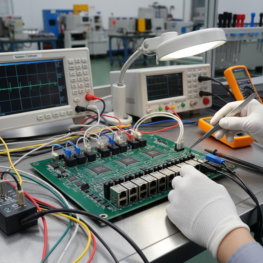
Testing multilayer PCBAs requires more than basic visual inspection. Because many connections are buried within the board, verification must combine multiple methods.
Multilayer PCBA Testing Overview
| Test Category | Purpose | Typical Focus |
|---|---|---|
| AOI | Verify component placement and solder quality | Dense SMT areas |
| X-ray Inspection | Check hidden joints and via integrity | BGA, QFN, multilayer vias |
| Electrical Testing | Confirm continuity and isolation | Inner-layer connections |
| Functional Testing | Validate real-world operation | Firmware-based validation |
| Thermal Stress Tests | Evaluate stability under heat | High-power or enclosed devices |
This layered testing approach reduces latent defects that could appear only after prolonged use.
6. Applications That Rely on Multilayer PCBA Manufacturing
Multilayer PCBAs are widely used across industries that demand compact design and reliable signal behavior.
Common application areas include:
-
Consumer electronics and smart devices
-
Camera systems and image processing boards
-
Industrial automation controllers
-
Communication and networking equipment
-
Power management and conversion modules
-
Embedded computing platforms
Each application places different demands on routing density, power handling, and signal integrity, which the manufacturer must support consistently.
7. What to Look for in a Multilayer PCBA Manufacturer
Choosing the right partner is critical when working with complex multilayer designs. Beyond basic capacity, buyers should evaluate how the manufacturer handles risk and consistency.
Key selection criteria often include:
-
Experience with medium-to-high layer count boards
-
Proven control over stack-up and lamination quality
-
Integrated inspection and testing capability
-
Ability to scale from prototype to volume production
-
Clear communication during design review and production
These factors determine whether a multilayer PCBA project moves smoothly or encounters costly delays.
Building Complex Electronics on a Stable Foundation
Multilayer PCBAs enable compact layouts, cleaner signals, and higher functional density—but only when fabrication and assembly are tightly controlled. A reliable multilayer PCBA manufacturer ensures that complexity translates into performance rather than risk.
To discuss multilayer PCBA requirements or explore assembly capabilities for complex electronic products, visit www.hcdpcba.com or contact the team directly through:
👉 https://www.hcdpcba.com/en/contact-us