Mastering High Bandwidth PCB Design for Next-Generation Applications
In the rapidly evolving world of electronics, high bandwidth PCB design stands as a pivotal innovation, enabling seamless data transfer and superior performance in demanding systems. At hcdpcba, we specialize in crafting these advanced solutions to meet the needs of industries pushing technological boundaries. Our expertise ensures that every board is optimized for speed and reliability, turning complex ideas into functional realities.
Understanding the Essentials of High Bandwidth PCB Design
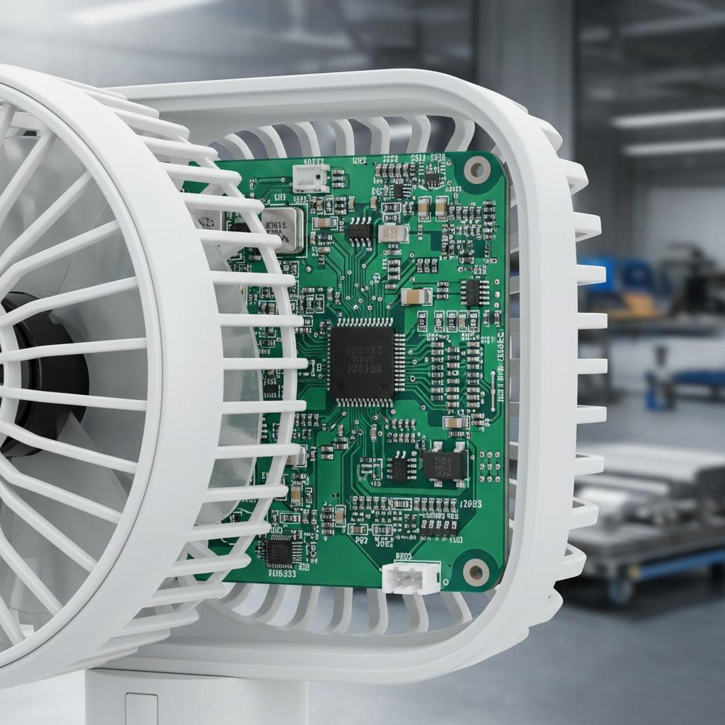
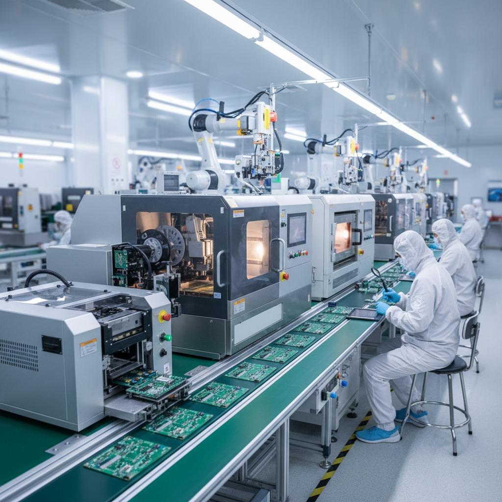
High bandwidth PCB design involves meticulous engineering to support elevated data rates without compromising signal integrity. Imagine a sleek, multi-layered board where traces are precisely routed to minimize crosstalk and electromagnetic interference, allowing signals to race through at gigabit speeds. This approach is crucial for applications requiring instantaneous processing, such as in data centers or high-speed networking equipment. At hcdpcba, our team leverages years of experience in multi-layer and HDI boards to deliver designs that handle frequencies up to several GHz. We incorporate advanced materials like high-frequency laminates, ensuring thermal stability and low loss, which vividly brings to life the backbone of modern computing infrastructures. By focusing on impedance control and differential signaling, our designs prevent data bottlenecks, painting a picture of effortless connectivity in even the most intricate setups.
Integrating PCB Design for AI Servers
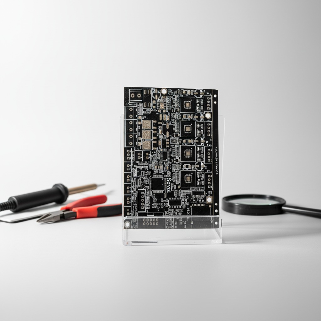
When it comes to PCB design for AI servers, the stakes are higher, demanding boards that can fuel the intense computational demands of artificial intelligence workloads. Picture a robust circuit like our SOYO 407-P2R27400A, with its array of microcontrollers and integrated circuits arranged in a harmonious black canvas, ready to orchestrate massive parallel processing. This board's multiple connectors and precisely placed capacitors and resistors optimize electrical flow, making it ideal for AI servers that process vast datasets in real-time. At hcdpcba, we tailor PCB design for AI servers to support high-density component integration, ensuring scalability for machine learning models that evolve daily. Our SMT patch services and PCBA customization allow for versatile interfaces, reducing setup time and enhancing productivity in AI-driven environments, from industrial automation to smart healthcare systems.
Why Choose hcdpcba for Your High Bandwidth Needs
Partnering with hcdpcba means accessing a suite of services that elevate high bandwidth PCB design to professional heights. Our PCB prototyping offers rapid turnaround with multi-layer precision, while our component sourcing, assembly, and testing ensure every board, including specialized ones for AI servers, meets rigorous standards. We provide DFMA analysis to streamline manufacturability, cutting costs without sacrificing quality, and our OEM/ODM capabilities deliver bespoke solutions for sectors like automotive electronics and IoT. With a commitment to confidentiality and swift response times, hcdpcba protects your innovations while driving efficiency. The SOYO 407-P2R27400A exemplifies our prowess, its labeled ports and robust layout vividly illustrating reliability in high-stakes applications.
Future-Proofing with Advanced PCB Solutions
Looking ahead, high bandwidth PCB design continues to shape the future of technology, particularly in PCB design for AI servers that power autonomous systems and edge computing. At hcdpcba, we're at the forefront, using our technical strengths to innovate with high-frequency boards that adapt to emerging trends. Envision servers humming with efficiency, their PCBs facilitating lightning-fast AI inferences that transform industries. Our quality controls guarantee zero defects, and cost optimizations make advanced tech accessible. Whether for communications or smart homes, our solutions ensure your projects not only perform but thrive, vividly capturing the essence of progress in electronics.