How an IoT Device PCBA Manufacturer Powers the Connected World
Every connected product—from a smart thermostat to a factory sensor node—depends on a circuit board that quietly handles signal accuracy, power efficiency, and environmental stress.
That circuit board is the product of an IoT device PCBA manufacturer, where electronics, materials science, and manufacturing discipline converge.
In this world, it’s not about how many boards are built—it’s about whether each one can connect, transmit, and survive. The following sections uncover how engineering precision transforms IoT design concepts into scalable, reliable hardware.
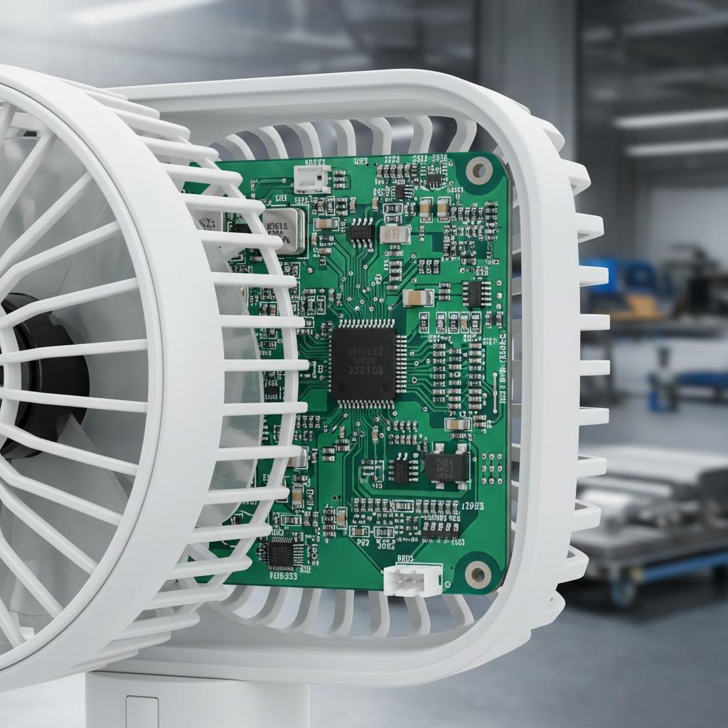
Design Foundations for the Internet of Things
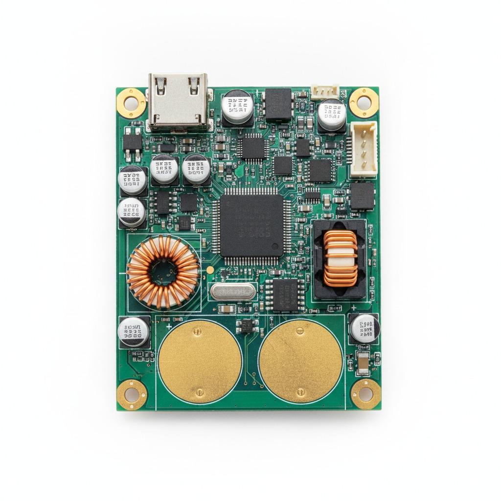
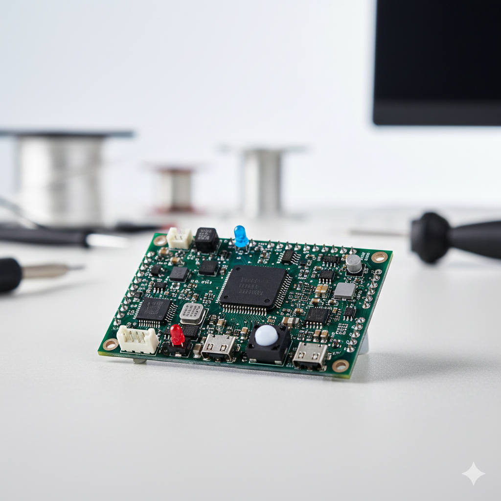
IoT boards face a paradox: smaller form factors, yet greater complexity.
Unlike consumer electronics, IoT PCBA design must balance connectivity, sensing, and power management while fitting inside limited enclosures.
Key design variables for smart IoT PCB assembly include:
| Design Element | Engineering Objective |
|---|---|
| Multi-Layer Stack-Up | Supports antenna isolation and signal routing for Bluetooth, Wi-Fi, or LoRa. |
| Low-Power Circuit Design | Extends battery life through optimized regulator and MCU sleep modes. |
| RF Layout Optimization | Ensures impedance matching and minimal signal loss for wireless modules. |
| Compact Form Factor | Allows integration into wearable and embedded systems. |
| Thermal Control & Shielding | Protects sensors and chips from heat or electromagnetic interference. |
The challenge is not just fitting components—but enabling communication reliability within milliseconds and microvolts.
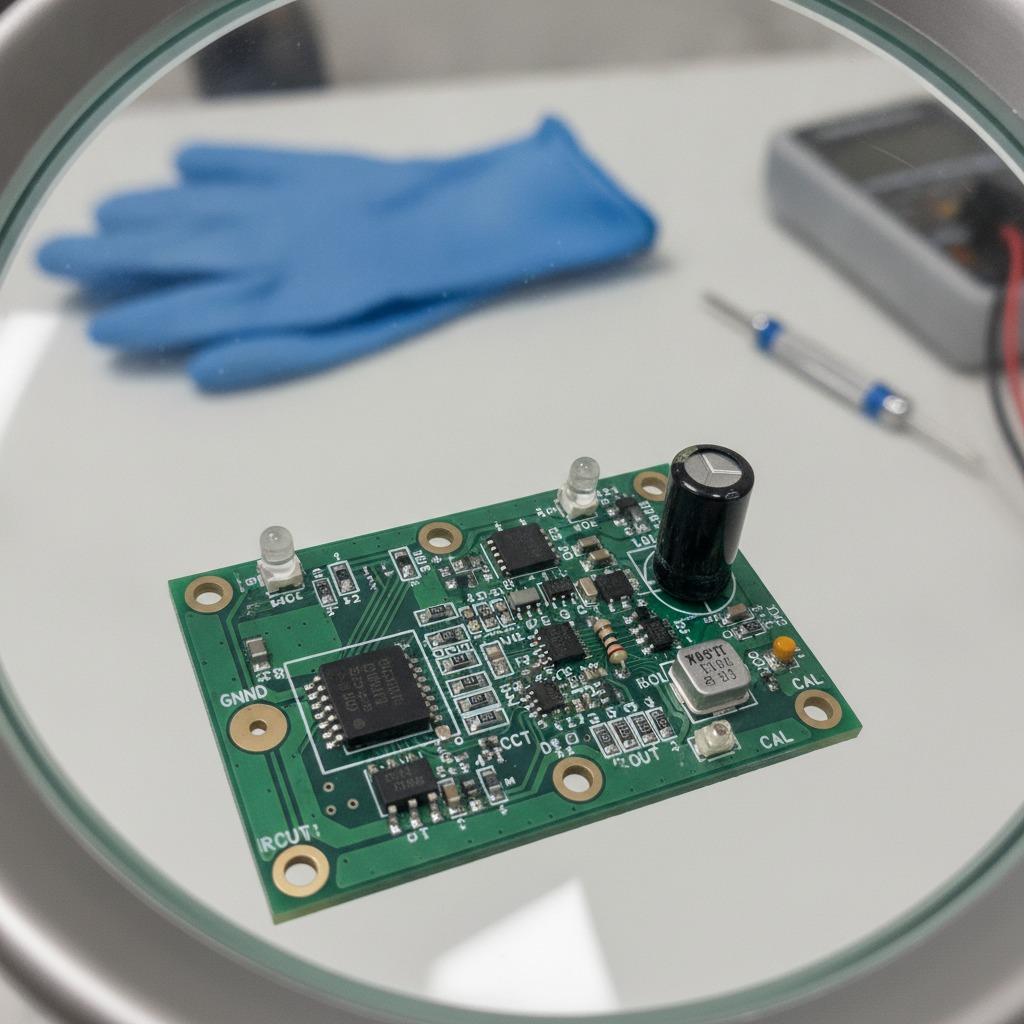
Wireless Module Integration: The Core of IoT Connectivity
The “intelligence” of any IoT device depends on how efficiently its modules—Wi-Fi, Bluetooth, Zigbee, NB-IoT, or LTE—are integrated and validated.
A capable IoT device PCBA manufacturer aligns mechanical design, RF testing, and antenna tuning from the earliest stages of layout.
Integration best practices include:
-
Pre-certified module selection to reduce regulatory risk.
-
3D antenna simulation to avoid detuning from metal housings.
-
Shielded ground planes to isolate digital noise from RF paths.
-
Automated RF calibration during end-of-line testing for consistent performance.
This fusion of electronics and RF engineering is what enables IoT boards to connect seamlessly, even in noisy environments.
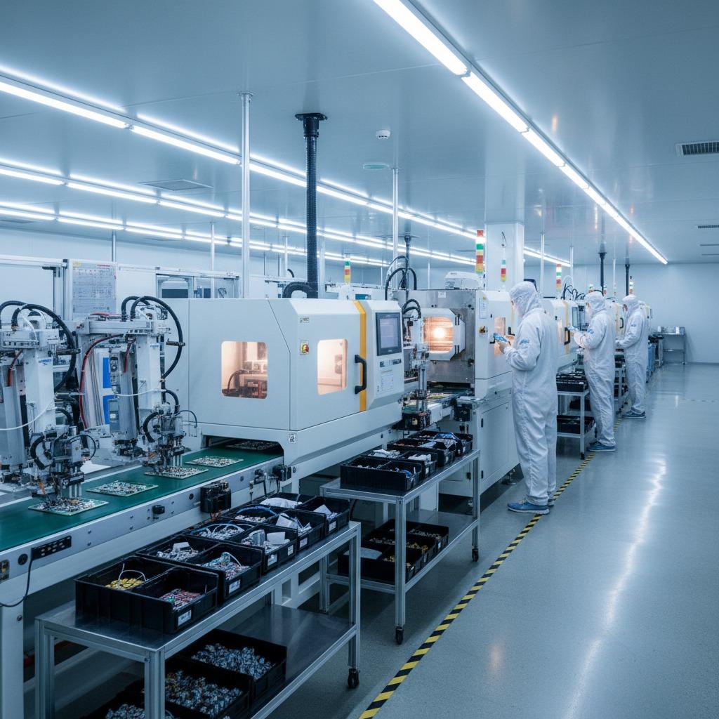
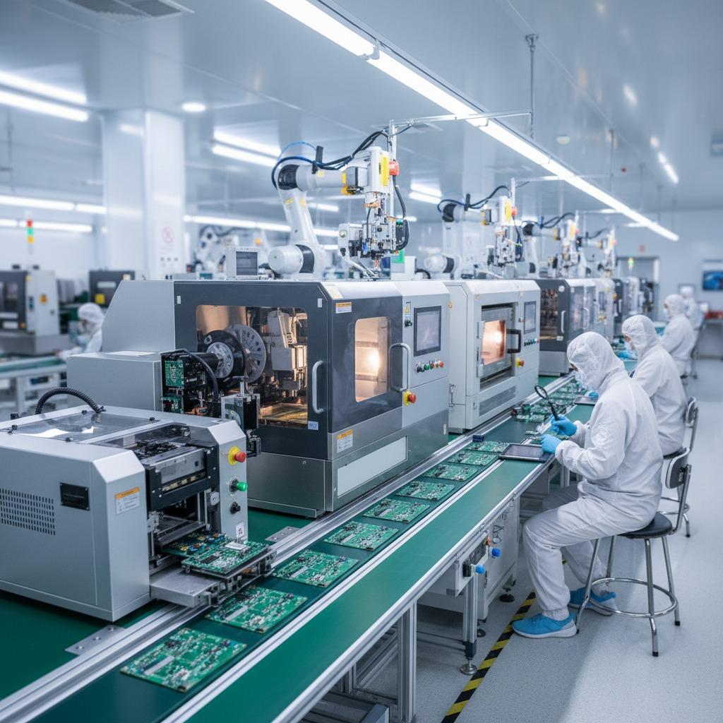
Turnkey PCBA Manufacturing for IoT Applications
A true IoT manufacturing partner doesn’t just assemble boards—it builds entire ecosystems.
In turnkey projects, material sourcing, firmware programming, and testing converge in one controlled environment.
| Manufacturing Stage | Purpose in IoT Production |
|---|---|
| Component Sourcing | Ensures certified and traceable wireless chipsets. |
| SMT + THT Integration | Supports complex module attachment with hybrid soldering. |
| Firmware Programming | Loads device-specific logic before functional testing. |
| Conformal Coating | Protects outdoor or industrial IoT devices against moisture. |
| Data Traceability | Records serial numbers and test results for each unit. |
This unified workflow prevents misalignment between design intent and mass production reality—something that fragmented suppliers often struggle with.
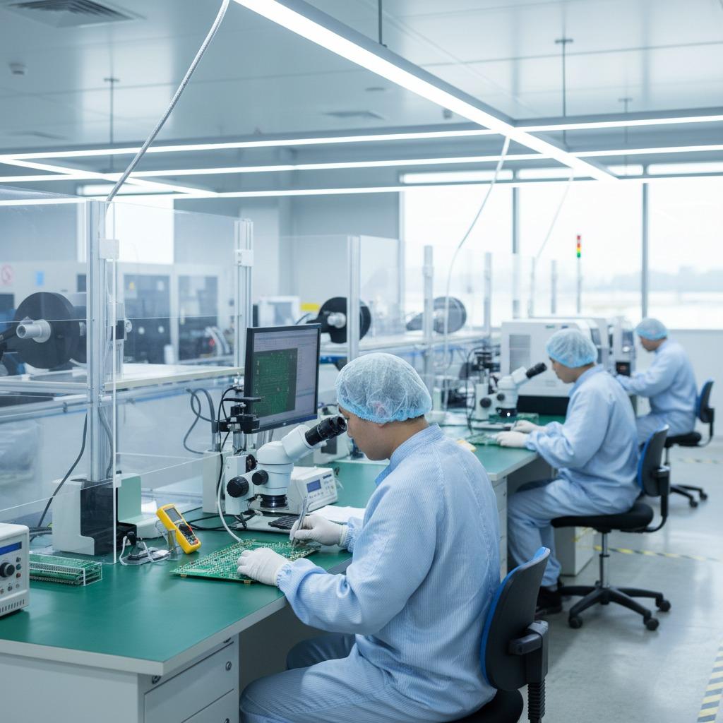
Reliability Testing: The True Benchmark for IoT Hardware
IoT boards must perform in unpredictable conditions—dust, humidity, vibration, and unstable power.
That’s why IoT reliability testing isn’t just quality control; it’s lifecycle validation.
Key testing procedures include:
-
Thermal Cycling (-40°C to +85°C) to evaluate solder fatigue and material expansion.
-
Vibration and Drop Simulation to ensure board rigidity inside mobile enclosures.
-
RF Performance Verification to validate antenna range and data throughput.
-
ESD and Surge Resistance for power and data interfaces.
-
Long-Duration Burn-In to reveal early failures before shipment.
Each test isn’t an expense—it’s a safeguard for brand trust in the connected world.
Selecting the Right IoT PCBA Partner for Your Application
Different IoT verticals demand different manufacturing capabilities.
Here’s how to align your project’s purpose with the ideal factory setup:
| IoT Application | Required Manufacturing Capability |
|---|---|
| Smart Home Devices | Compact high-density PCBA with RF shielding and low-noise layout. |
| Industrial IoT Sensors | Wide temperature materials, conformal coating, and IPC Class 3 standards. |
| Wearables & Health Tech | Flexible PCB handling, lightweight materials, and medical-grade solder control. |
| Smart Agriculture / Outdoor Systems | Waterproofing, corrosion protection, and UV-resistant coatings. |
| Automotive Connectivity Modules | EMI-resistant design and vibration-certified testing. |
Selecting your IoT device PCBA manufacturer isn’t about geography—it’s about process maturity and environmental adaptability.
Engineering the Future of Connectivity
IoT is not a single technology—it’s a convergence of disciplines.
Behind every smart sensor or connected gateway lies a factory that understands the balance between performance, miniaturization, and manufacturability.
The best manufacturers don’t just build hardware—they enable reliability at scale.
If you’re developing IoT hardware that requires precision, integration, and verified durability, explore our production capabilities at our homepage.
For detailed engineering consultation, you can reach our technical team directly via the contact page.
Together, we can make your devices more connected—and more dependable.