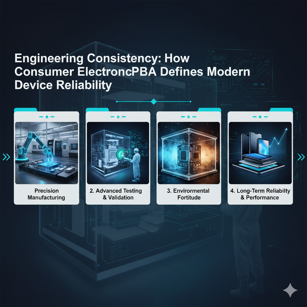
How Consumer Electronics PCBA Defines Modern Device Reliability
Consumer electronics has evolved from simple circuitry to complex ecosystems of high-density components, wireless modules, and embedded intelligence.
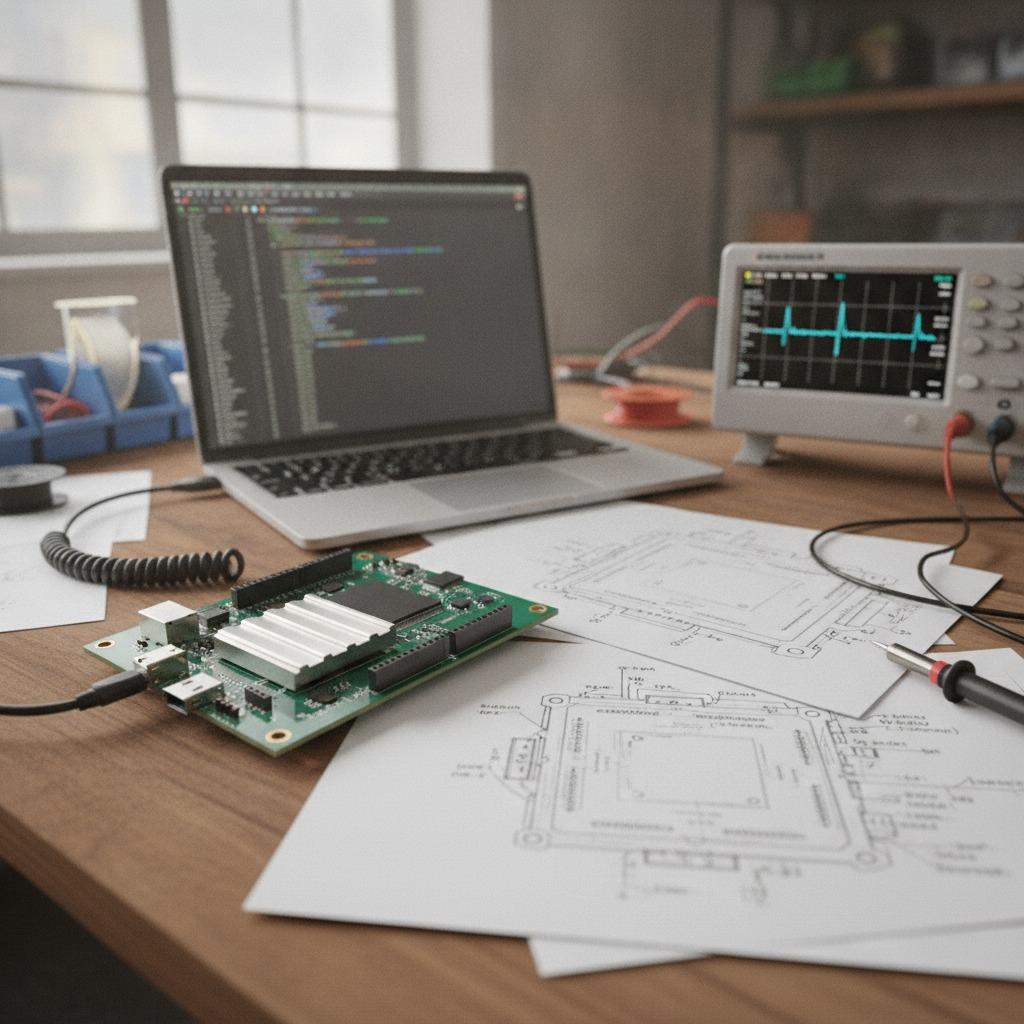
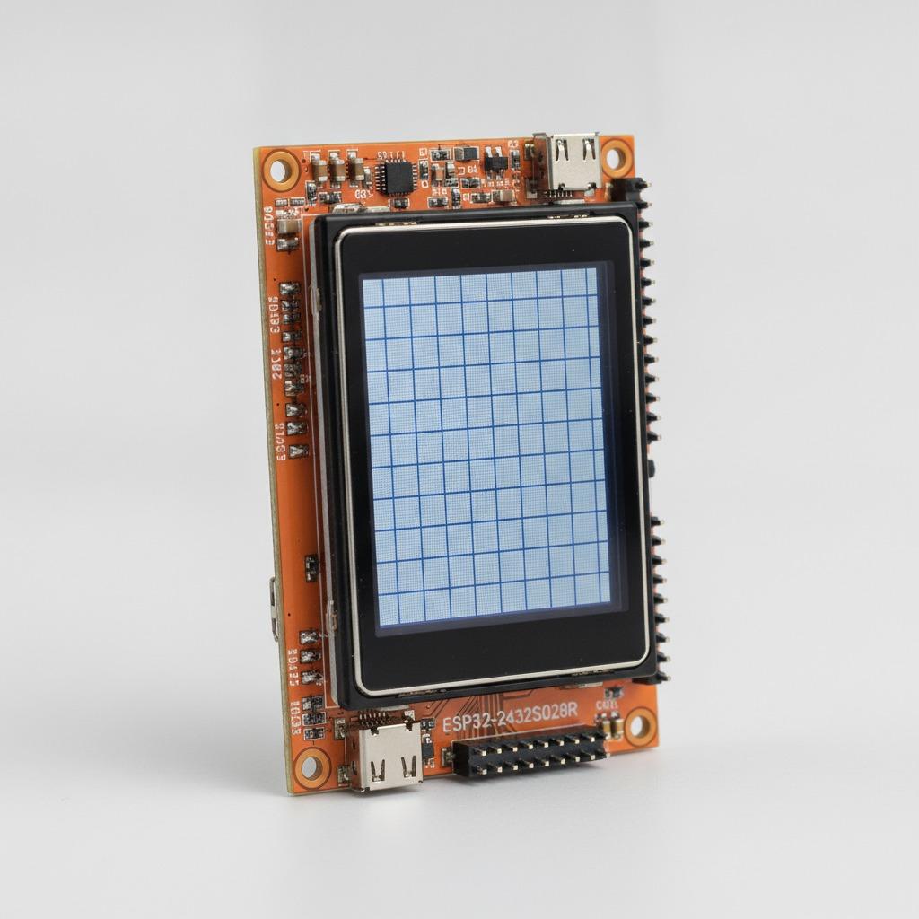
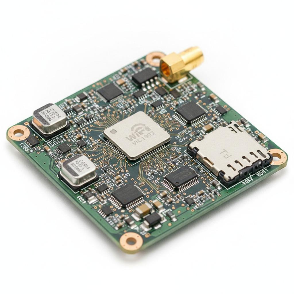
At the core of every device—from smartphones and wearables to smart speakers and projectors—lies the consumer electronics PCBA, a system that transforms digital logic into physical functionality.
Yet reliability isn’t born from innovation alone. It emerges from disciplined engineering—how precisely the PCBA is designed, assembled, and tested. Let’s explore how advanced process control and component design determine the real performance behind modern electronics.
Design Density and Its Hidden Engineering Challenges
The race toward miniaturization brings tighter tolerances, thinner boards, and higher heat concentration.
In a high-density PCB assembly, signal integrity and thermal management become competing priorities.
Manufacturers must balance component proximity, copper thickness, and via distribution to prevent crosstalk and hotspot failure.
Key engineering considerations include:
| Design Factor | Impact on Reliability |
|---|---|
| Trace Width & Spacing | Influences impedance control and EMI performance. |
| Via-in-Pad Design | Reduces routing complexity but requires precise filling and planarization. |
| Thermal Relief Optimization | Prevents pad lifting during reflow and uneven solder joints. |
| Component Orientation & Symmetry | Minimizes shadowing during reflow and balances solder wetting. |
| Layer Stack-Up Design | Affects heat dissipation and long-term board warpage control. |
Design is where most hidden risks originate—and where the best PCBA manufacturers intervene early through DFM (Design for Manufacturability).
SMT Process Control for High-Speed Consumer Electronics Production
Once design is frozen, the challenge shifts to consistency—every second on the production line counts.
For mass production PCBA, a single deviation in stencil printing or reflow temperature can multiply into hundreds of defects.
To counter this, mature consumer electronics manufacturing partners deploy full automation with active feedback systems:
-
SPI (Solder Paste Inspection) detects print volume variations in real time.
-
AOI (Automated Optical Inspection) corrects placement offset and solder bridging.
-
Smart Feeder Systems track component usage and prevent feeder drift.
-
Reflow Profiling Sensors monitor zone temperatures across every batch.
Process control here isn’t about speed—it’s about predictability. Every board produced at 3 AM should match the quality of one made at noon.
Material Selection and Assembly Methods for Smart Devices
The miniaturization of smart device circuit boards has increased the demand for lightweight, low-warpage, and thermally stable materials.
Factories often combine FR-4 with polyimide or halogen-free laminates, paired with selective gold plating for fine-pitch connectors.
Assembly techniques also vary:
| Assembly Type | Use Case | Key Advantage |
|---|---|---|
| Reflow Soldering (SMT) | Smartphones, wearables | High-speed precision for mini components. |
| Selective Wave Soldering | Mixed TH + SMT boards | Prevents solder splash and thermal stress. |
| Press-Fit Assembly | Audio and automotive boards | Improves mechanical connection without solder. |
| Conformal Coating | Outdoor consumer devices | Protects against humidity and dust ingress. |
Each assembly choice is a compromise between function, cost, and environmental reliability.
Reliability Testing: Making Consumer Electronics Survive the Real World
A high-yield production run means nothing without proven durability.
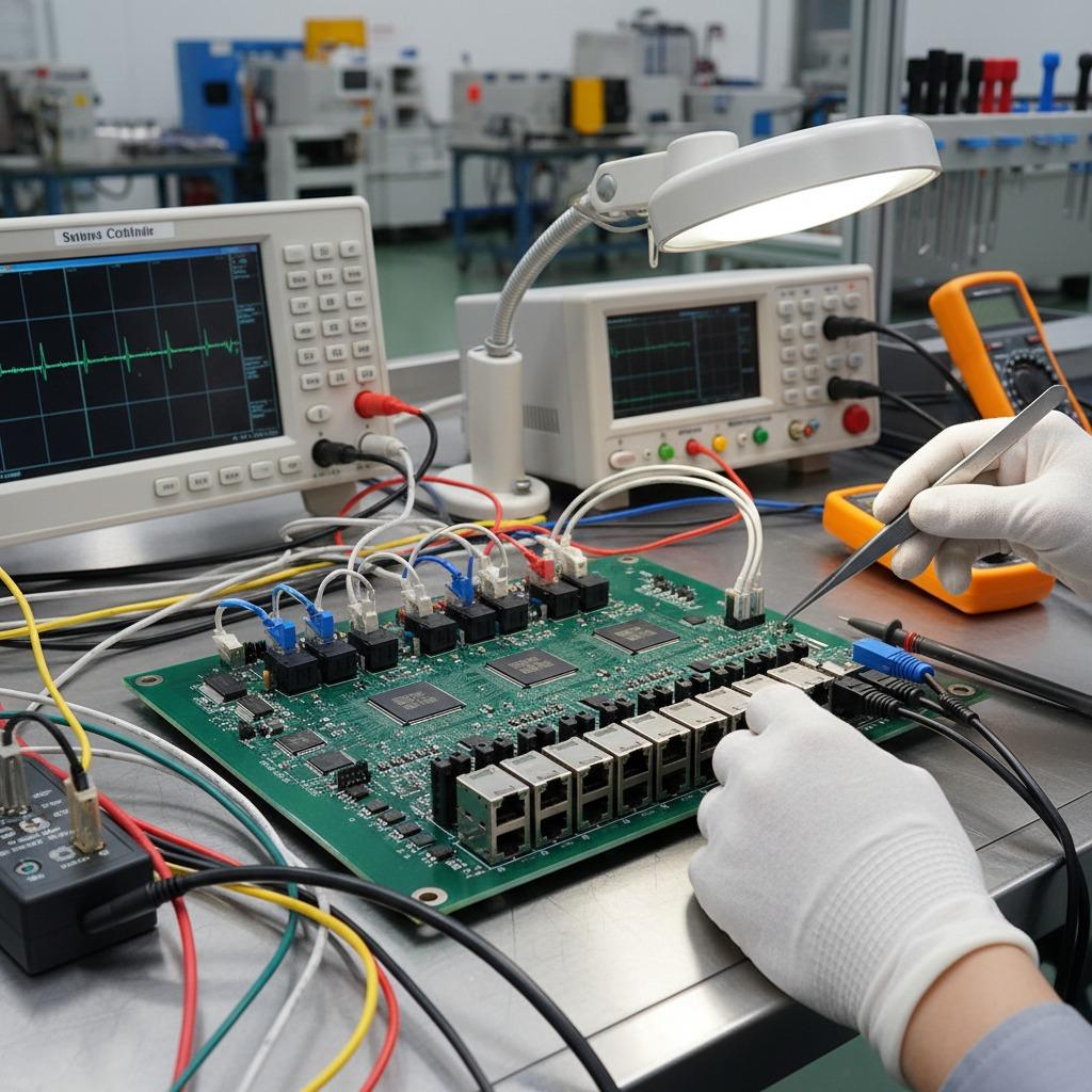
Professional reliability testing PCBA programs simulate the real-world stress your product will face.
Testing goes beyond visual inspection—it’s a data-driven evaluation of long-term endurance.
Typical test coverage includes:
-
Thermal Shock and Cycling: Evaluates solder fatigue and material expansion.
-
Vibration and Drop Tests: Verifies mechanical resilience of BGA and QFN components.
-
Humidity and Salt Spray: Detects corrosion resistance in wearable and outdoor devices.
-
Functional Burn-In: Identifies early failures before shipment.
These tests validate that your board isn’t just assembled—it’s qualified for life in the consumer market.
Choosing a PCBA Partner That Matches Your Product’s Scale
Every consumer electronics brand faces different priorities: startups need design agility, while established brands demand repeatability.
Here’s how to align your needs with the right turnkey electronics assembly partner:
| Project Stage | What to Look For in a Factory |
|---|---|
| Prototype / Pilot Run | Fast DFM feedback, on-site engineering adjustments, flexible lot size. |
| Mass Production | Multi-line scheduling, yield tracking system, and process data transparency. |
| New Product Launch (NPI) | Dedicated engineering support for ECN management and testing fixture design. |
| Product Refresh / Upgrade | BOM optimization and cross-component validation for cost reduction. |
Before outsourcing, verify whether your supplier can provide test data, process documentation, and traceable lot reports—not just a quote.
From Miniaturization to Mass Scale: Engineering That Sustains Growth
As consumer electronics evolve toward smarter, thinner, and faster devices, the consumer electronics PCBA has become the core of innovation and stability.
The manufacturers that master balance—between density and dissipation, speed and control—are the ones who define tomorrow’s reliability standards.
To explore how our PCBA systems deliver high-precision assembly and full reliability testing for smart devices, visit our official website.
For technical consultation or project evaluation, reach our engineers directly via the contact page.
Your next innovation deserves an assembly partner built for precision.