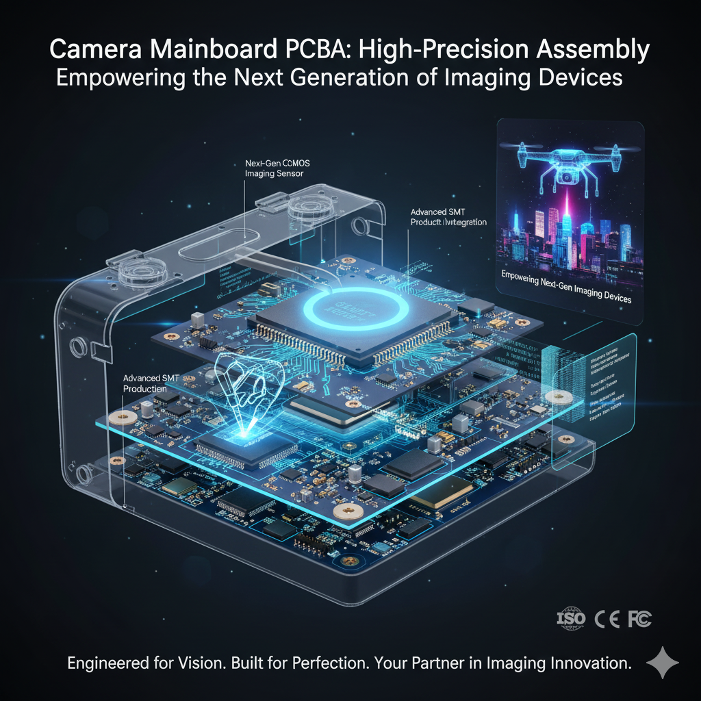
Camera Mainboard PCBA: High-Precision Assembly Empowering the Next Generation of Imaging Devices
Every pixel of image clarity originates from a circuit board.
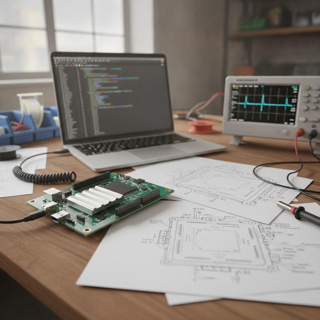
Inside every security camera, dash cam, medical imaging system, and industrial vision sensor lies a camera mainboard PCBA—a high-density, high-frequency electronic heart that captures, converts, and transmits visual data.
For manufacturers, this board is where optics meet electronics, where signal timing meets heat management.
It determines not only how a camera functions, but how it performs over time—frame by frame, in every light condition.
Core Role of Camera Mainboard PCBA in Modern Imaging Systems
The camera mainboard integrates all critical functional blocks: sensor interface, image signal processor (ISP), power delivery, communication, and synchronization control.
Each subsystem demands tight manufacturing precision to ensure color accuracy, noise reduction, and operational stability.
| Subsystem | Function | PCBA Engineering Focus |
|---|---|---|
| CMOS Sensor Interface | Captures analog light data | MIPI/LVDS impedance control ±5% |
| ISP Module | Converts and enhances digital image | Ground isolation, EMI shielding |
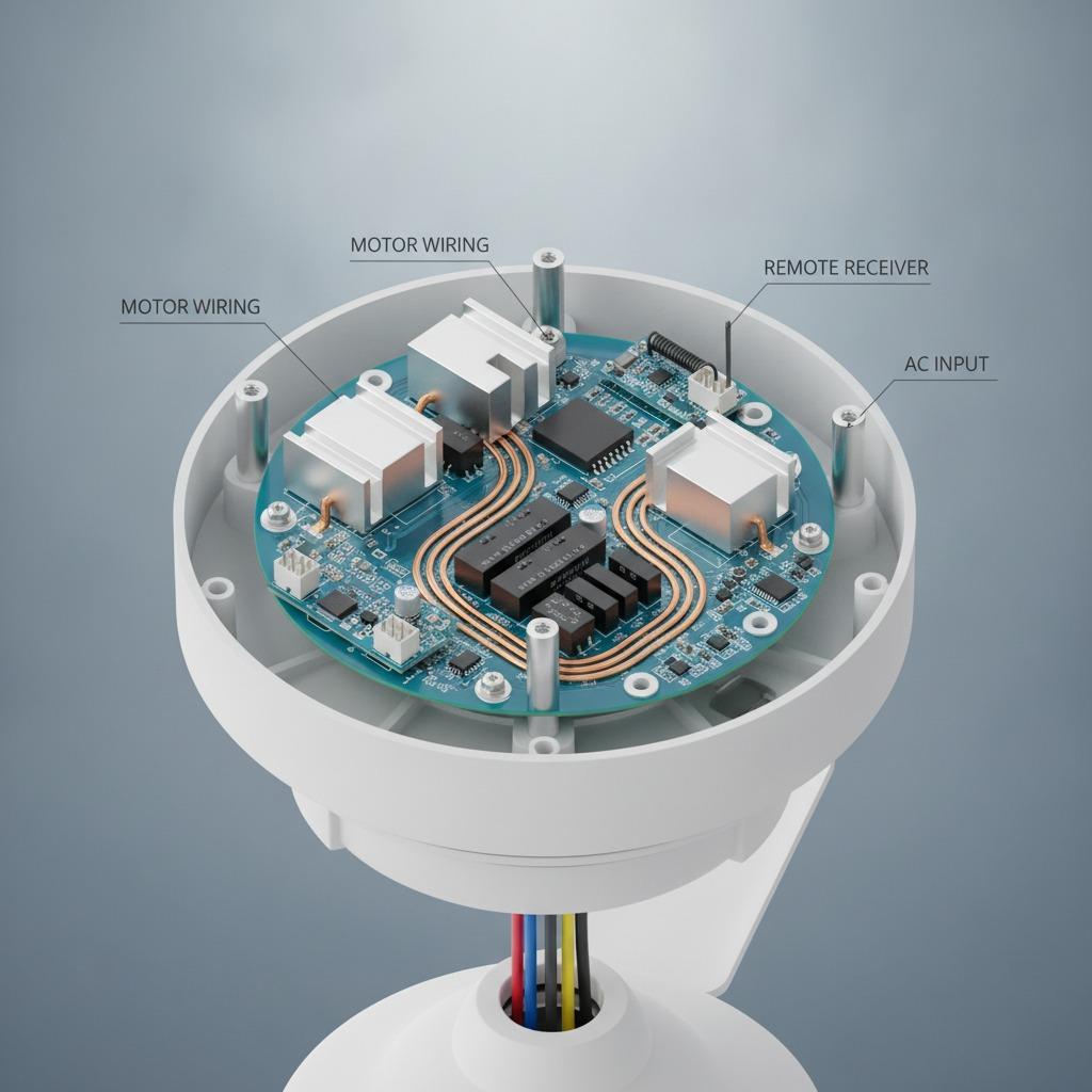
| Lens & Motor Control | Focus, zoom, and aperture adjustment | PWM precision, current isolation |
| Power Management | Supplies multi-level voltage rails | Low ripple (<30mV) and surge protection |
| Data Transmission | Outputs image data | HDMI, USB, or Ethernet impedance consistency |
| Clock Control | Synchronizes exposure and frame rate | Phase jitter <50ps |
Each circuit node directly affects image stability and resolution consistency—especially in automotive, machine vision, or medical applications that require pixel-perfect data.
Advanced PCB Design for High-Frequency Signal Stability
A camera’s data bus must transmit several gigabits of information per second.
That requires high-frequency signal routing techniques, combining precision layout with advanced materials.
Professional manufacturers apply:
-
8–12 layer stack-ups to separate analog, digital, and power domains.
-
Low-loss dielectric materials such as FR-408HR or Rogers 4350B to minimize signal delay.
-
Differential pair routing for MIPI, LVDS, and HDMI signals with matched lengths within ±3mil.
-
Blind and buried vias to compact complex routing without increasing board thickness.
-
Shielded ground planes between analog and digital layers to suppress crosstalk and EMI.
Each trace behaves like a transmission line.
A single impedance mismatch can cause reflection and degrade the final image quality—something only precision-controlled PCB design can prevent.
Optical-Grade Assembly for CMOS and Lens Alignment
The CMOS sensor is the most sensitive component on the board.
Its placement accuracy directly determines the optical axis and focus consistency of the camera module.
To guarantee this precision, camera mainboard PCBA factories integrate optical-grade processes:
-
Vacuum-assisted pick-and-place for BGA and sensor components to avoid micro-vibration misalignment.
-
Temperature-gradient reflow soldering, maintaining under 2°C variation across the PCB to prevent warping.
-
Optical alignment verification systems to calibrate sensor-to-lens offset after reflow.
-
Cleanroom co-assembly of PCBA and optical module to avoid contamination that affects image clarity.
-
Custom jigs and fixtures designed for each sensor model to maintain mechanical and optical consistency.
This meticulous alignment process ensures the optical and electrical centers align perfectly—essential for autofocus, HDR, and low-light performance.
Thermal and Power Control: Keeping Image Quality Stable
A camera’s ISP and processor generate concentrated heat during operation.
If not managed properly, this can cause image noise, frame drops, or even sensor degradation.
Thermal management features integrated into the PCBA include:
-
Copper pours and heat vias under power and ISP zones for rapid dissipation.
-
Thermal pad interfaces for SoC packages with dedicated metal backplates.
-
Aluminum or metal-core substrates for high-power camera designs.
-
Smart temperature feedback circuits integrated with firmware to throttle operation dynamically.
-
Conformal coating for environmental resistance in outdoor or automotive-grade cameras.
Through precise heat mapping and design iteration, these thermal optimizations maintain stable voltage and color balance—even under 24/7 operation.
Manufacturing Process: Precision Beyond Assembly
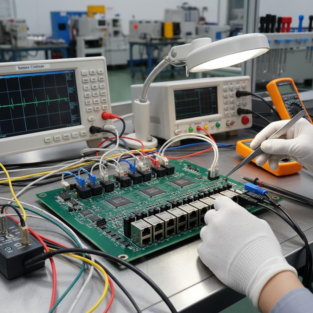
A professional camera PCB assembly line is built around traceability and consistency.
From material preparation to post-production testing, every step ensures process integrity.
| Manufacturing Step | Key Control Metric | Purpose |
|---|---|---|
| Solder Paste Printing | Thickness tolerance ±10µm | Prevents bridging at fine-pitch ICs |
| High-Speed Placement | ±25µm accuracy for 0201–BGA | Guarantees sensor pin integrity |
| Nitrogen Reflow Soldering | 7–9 zone temperature profile | Minimizes oxidation and voids |
| AOI + X-ray Inspection | 100% inline coverage | Detects hidden joint or alignment issues |
| In-Circuit Test (ICT) | Continuity and power validation | Ensures stable power supply rails |
| Functional Test (FCT) | Image, focus, color response | Simulates real imaging conditions |
Every production cycle is data-logged under MES supervision, providing complete traceability and reproducibility across batches.
Key Advantages of Professional Camera Mainboard PCBA Manufacturing
Choosing an experienced camera mainboard PCBA manufacturer ensures more than reliable assembly—it delivers engineering value throughout your product lifecycle.
Core advantages include:
-
Cross-domain expertise — integration of electrical, optical, and mechanical design.
-
High-speed production capability — simultaneous builds for multiple camera models.
-
Automated inspection systems — AOI, X-ray, and functional imaging verification.
-
Stable quality across environments — automotive-grade materials and process standards.
-
Scalable customization — tailored board layouts, connectors, and control logic for each camera platform.
This blend of precision, flexibility, and scalability enables faster market launch and long-term reliability.
Applications Across Industries
Camera mainboard PCBAs are not limited to consumer imaging—they power multiple verticals:
-
Automotive cameras (ADAS, parking assist, dash cams) requiring vibration resistance.
-
Industrial vision for robotics and production line inspection.
-
Smart home systems such as doorbell and surveillance cameras.
-
Medical imaging devices with high-resolution sensors for diagnosis.
-
Broadcast and drone cameras demanding ultra-low latency and dynamic range.
Each application imposes its own mechanical, environmental, and electrical demands—handled through precision-tailored PCBA solutions.
From Board to Vision: The Foundation of Image Clarity
Every sharp, stable image starts from a reliable foundation—a well-engineered camera mainboard PCBA.
It’s where electrons turn into visuals, and manufacturing precision becomes image quality.
If your next imaging product requires advanced board design, high-frequency signal control, and sensor-level precision, visit www.hcdpcba.com to explore our capabilities.
For technical consultation or prototype evaluation, contact our engineers via the contact page.
Because true vision starts at the board level—and precision defines every frame.