AI Device PCBA Factory: Building the Core Boards that Power Intelligent Hardware
Artificial intelligence is only as capable as the hardware it runs on.
Behind every edge AI camera, smart sensor, or robotics controller lies a carefully engineered AI device PCBA—the true foundation of machine intelligence.
A professional AI device PCBA factory isn’t just soldering chips; it’s enabling real-time processing, power stability, and seamless connectivity under heavy computational loads.
In this environment, electrical precision becomes the new performance metric.
How PCBA Shapes AI Hardware Performance
An AI system’s performance is often limited not by the algorithm, but by how its circuit board handles speed, heat, and power.
The complexity of AI hardware PCB assembly lies in balancing three forces—high-frequency signal routing, thermal control, and multi-chip synchronization.
| AI Hardware Function | PCBA Engineering Focus | Manufacturing Challenge |
|---|---|---|
| Neural Compute Module | Dense BGA and SoC placement | Tight pitch reflow control |
| Power Management | High-current low-noise conversion | Multi-layer copper balancing |
| Data Interface Section | High-speed USB/PCIe routing | Controlled impedance ±5% |
| AI Accelerator Board | FPGA + GPU mounting | Thermal dissipation and solder joint reliability |
| Sensor Interface | Analog/digital isolation | Noise suppression and grounding design |
Each section requires a unique set of tolerances and manufacturing precision.
The smallest deviation in signal integrity can mean milliseconds lost—or models failing to infer correctly.
High-Speed and High-Density PCB Design
AI hardware boards typically run data buses exceeding 10Gbps.
Such speed demands strict high-speed data PCB design, where even a 0.1mm trace offset can alter impedance.
To maintain signal quality, factories deploy:
-
Multi-layer PCBs (8–16 layers) with ground-reference pairs for differential routing.
-
Laser-drilled microvias for compact interlayer connection.
-
Impedance-controlled inner layers within ±5% tolerance.
-
Low-loss dielectric materials (FR-408, Rogers 4000 series) for minimal signal delay.
-
Automated optical alignment systems to ensure via-to-pad accuracy within 25µm.
These methods ensure that AI data flows without reflection, loss, or latency—critical for neural inference efficiency.
Thermal and Power Stability for AI Modules
AI processors generate significant heat under continuous load.
A true AI device PCBA factory integrates both electrical and mechanical design to keep systems within thermal limits.
Key strategies include:
-
Copper pours and thermal vias to conduct heat away from BGAs.
-
Hybrid cooling combining PCB metal core and external heat sink interfaces.
-
Power integrity simulation to prevent voltage droop under high current draw.
-
Automated thermal profiling during reflow for uniform solder wetting.
-
Conformal coating to protect against moisture and oxidation in high-temperature environments.
These steps ensure the AI board performs consistently even in industrial robotics, autonomous systems, and edge computing devices.
Edge AI and Modular PCBA Integration
Modern applications don’t always use centralized processors.
Edge AI modules integrate compute and communication within a compact edge AI module PCBA, requiring modular, stackable architecture.
Professional AI PCBA lines are equipped for:
-
MCM (Multi-Chip Module) integration with AI accelerator + storage + WiFi modules.
-
Precision SMT placement for 01005 components on dense boards.
-
Multi-board interconnects (board-to-board, mezzanine connectors).
-
Custom AI circuit manufacturing to meet varying voltage and bandwidth needs.
This modular flexibility allows hardware developers to scale easily—from one prototype to full product series—without redesigning the board from scratch.
Testing and Quality Control for Neural Computing Boards
AI boards demand more than functional testing—they require performance validation.
In advanced neural computing board manufacturing, the testing process ensures both electrical reliability and computational consistency.
| Testing Stage | Purpose | Methodology |
|---|---|---|
| AOI + X-ray | Detect solder voids or misalignment | Inline automated optical inspection |
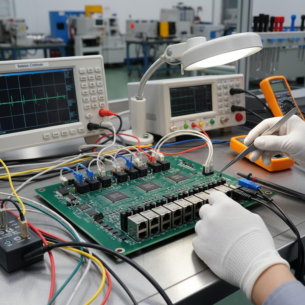
| High-Speed Signal Test | Verify PCIe, USB, and DDR links | Oscilloscope-based eye diagram check |
| Thermal Stress Test | Validate sustained load performance | Chamber simulation 85°C/24h |
| Functional AI Inference Test | Confirm SoC + GPU + memory integration | Model execution benchmark |
| Burn-in Reliability | Detect latent solder fatigue | 100-hour continuous power test |
Testing isn’t an afterthought—it’s the proof that complex electronic intelligence can endure real-world environments.
Manufacturing the Intelligence of Tomorrow
From wearable AI assistants to autonomous machines, every intelligent device starts with one foundation—a reliable, high-speed, and thermally stable AI device PCBA.
Partnering with a professional factory ensures not only product functionality, but also scalability, consistency, and compliance with the latest standards.
If your next AI hardware project requires performance-grade PCBA manufacturing, explore our solutions at our homepage.
For consultation or project discussion, connect with our engineering team via the contact page.
Because real intelligence begins at the board level.