What Should an IoT PCBA Manufacturer Actually Deliver?
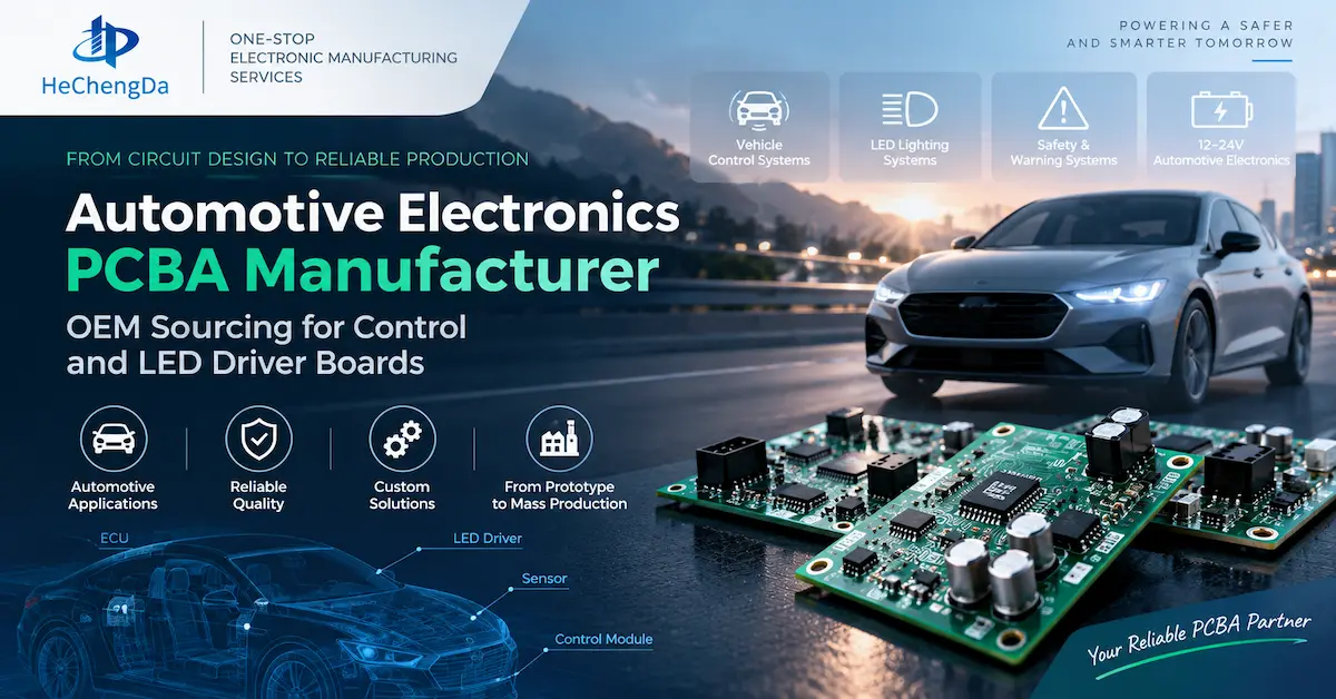
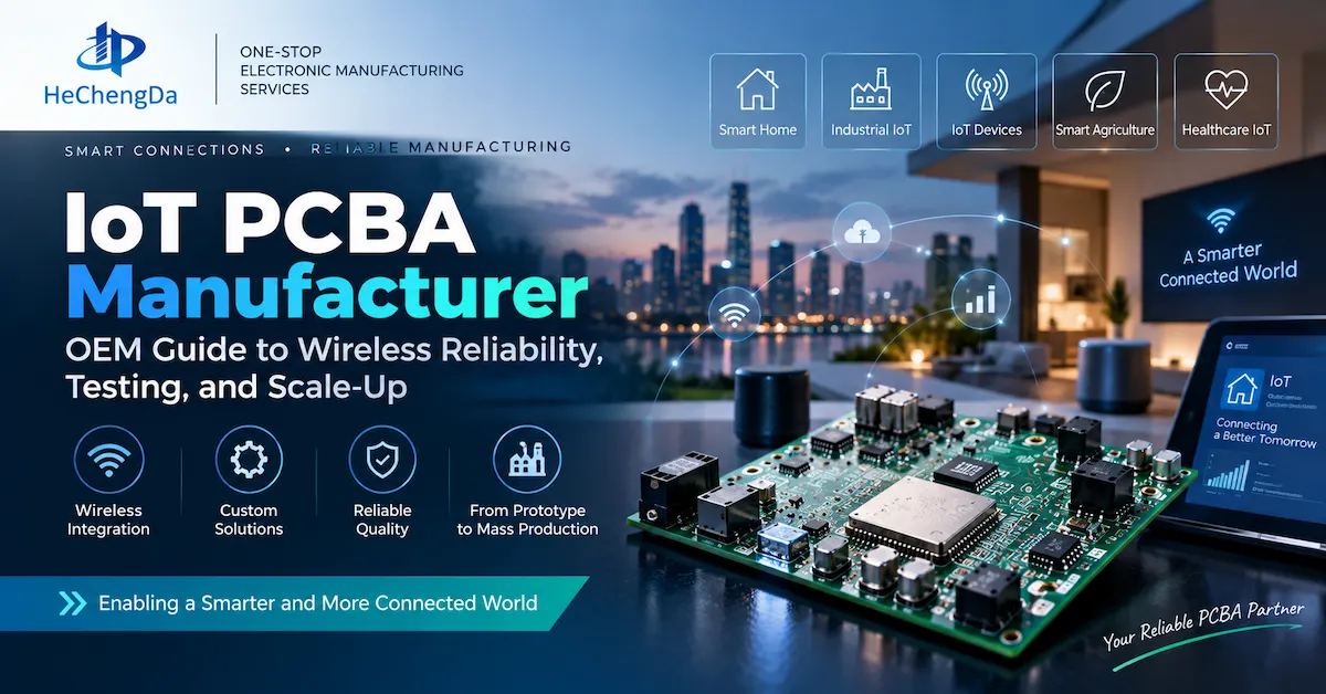
An IoT PCBA manufacturer should do more than place components onto a printed circuit board. Connected products combine processing, sensors, wireless communication, power management, firmware, and physical interfaces in a compact system, so the manufacturing requirement extends from PCB manufacturability and component sourcing to assembly consistency, programming, inspection, functional verification, and controlled repeat production. HCDPCBA positions its services around PCB prototyping, SMT assembly, customized PCBA, component sourcing, DFMA, testing, and OEM/ODM manufacturing, while IoT is listed among the industries it serves. Buyers developing smart sensors, gateways, home automation products, monitoring devices, or other connected electronics can therefore start with HCDPCBA's IoT PCB assembly services, but the final manufacturing scope should always be defined by the actual design files and acceptance requirements rather than a general IoT label.
Which Buyers Need an IoT PCBA Manufacturer—and When Is a Simple Assembly Quote Not Enough?
An IoT PCBA manufacturer is relevant to smart-device brands, IoT startups, industrial equipment companies, security-product manufacturers, smart-home companies, electronics design houses, and OEMs moving connected hardware from prototype to repeat production. A simple build-to-print quotation may be sufficient when the PCB design, BOM, firmware, test method, and production documents are already released; a turnkey PCBA route becomes more useful when the buyer also needs component sourcing and production coordination; ODM involvement is more appropriate when substantial engineering development remains unresolved. Buyers should not request a mass-production price when critical wireless, power, mechanical, or firmware requirements are still undefined, because the quotation will inevitably depend on assumptions. HCDPCBA's one-stop electronics manufacturing scope provides a useful starting point for defining which stages can be included in the project.
Start With the IoT Application Before Discussing PCB Assembly
The manufacturing plan should begin with where and how the connected product will operate. A battery-powered environmental sensor may prioritize low standby current and repeatable sleep/wake behavior; a smart-home controller may combine wireless connectivity, sensor inputs, relays, or display interfaces; an industrial monitoring node may require stable communication and reliable connectors inside equipment that operates for long periods; a gateway may need several interfaces and more complex power management. HCDPCBA currently presents application directions including Smart Home IoT PCB assembly, Consumer IoT PCB Assembly, and wireless communication boards. These pages demonstrate the breadth of connected-device applications, but they should not be interpreted to mean every IoT project uses the same wireless protocol, processor, antenna, environmental specification, or testing procedure.
Build an IoT PCBA Requirement Sheet Before Requesting a Quote
A professional RFQ should translate product expectations into manufacturing information. Instead of telling an IoT PCBA manufacturer that the board needs “Wi-Fi,” “low power,” or “industrial reliability,” define the required module or chipset where it has already been selected, power source, operating modes, interfaces, sensors, programming requirements, mechanical limits, antenna arrangement, and acceptance tests. The table below is a buyer-side specification framework rather than a published specification for every HCDPCBA IoT board, because custom PCBA requirements vary from project to project.
| Requirement Area | What the Buyer Should Define | Why It Affects Manufacturing |
|---|---|---|
| IoT application | Sensor, gateway, smart control, security, monitoring, wearable or other device | Establishes operating and verification priorities |
| Wireless system | Selected module/chipset, protocol, antenna method and interface requirements | Influences placement, RF-sensitive areas and testing |
| Power architecture | Input source, battery or adapter, regulators, operating modes and power targets | Affects component choice, thermal behavior and functional testing |
| Processor/control | MCU, processor, memory and required programming | Determines sourcing, package handling and firmware steps |
| Sensors/interfaces | Sensor types, USB, UART, I²C, SPI, Ethernet or project-specific interfaces | Defines connectivity and functional-test requirements |
| PCB construction | Dimensions, layer stack, material, copper, finish and controlled-impedance requirements where applicable | Defines fabrication requirements |
| Mechanical limits | Board outline, mounting holes, connectors, antenna clearance and component-height limits | Determines enclosure compatibility |
| Firmware | Version, programming file, programming method and device-specific data | Requires controlled software handling |
| Testing | Electrical, functional, connectivity and project-specific acceptance requirements | Defines fixture, test time and shipment criteria |
| Production control | Revision, serial/batch identification, packaging and change approval | Supports repeat-order consistency |
Control Wireless Modules, Sensors, and Critical BOM Items
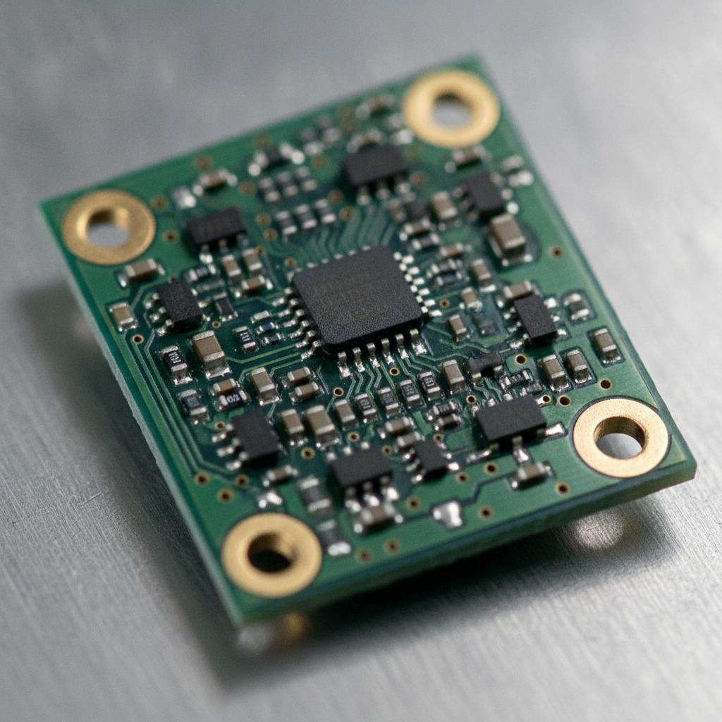
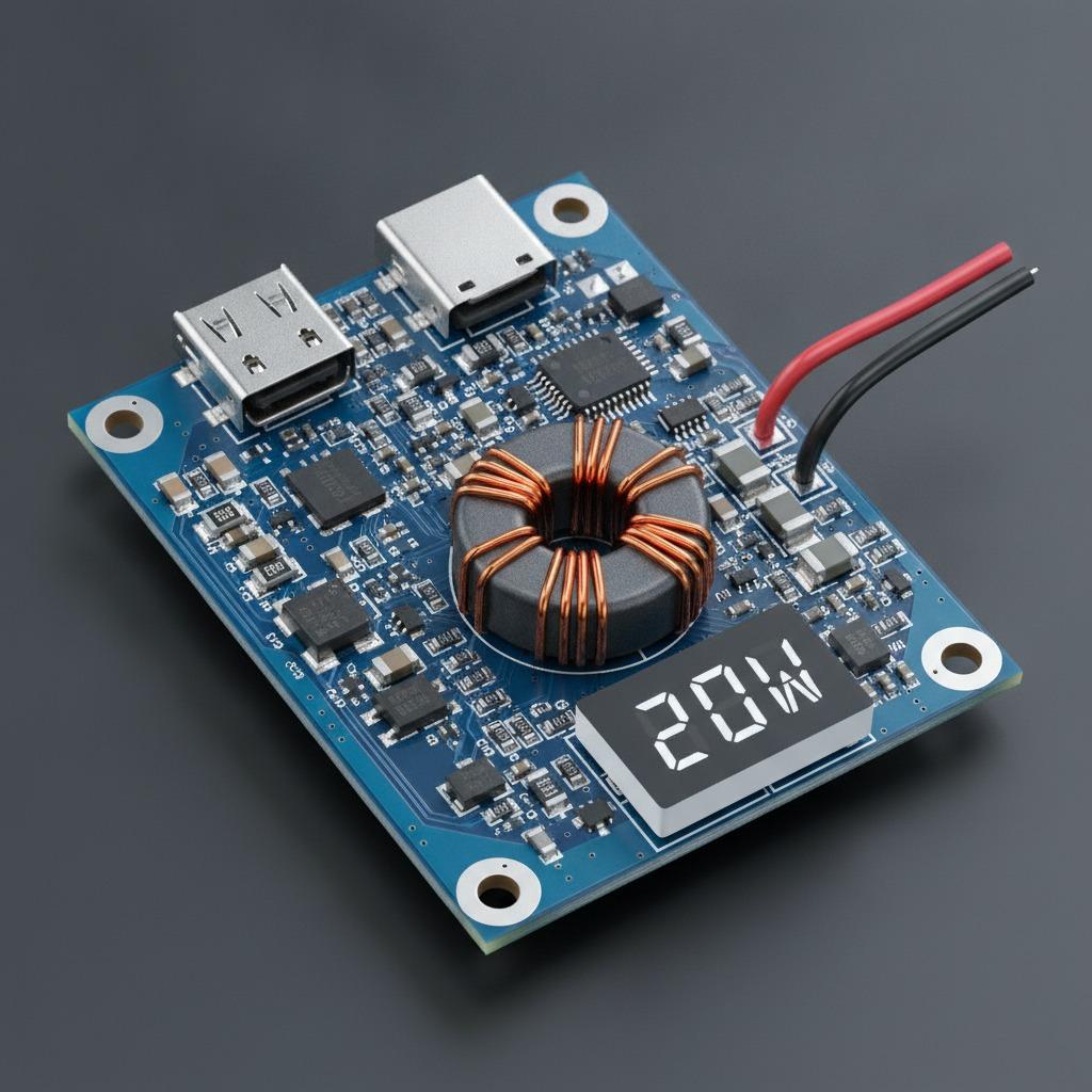
Component management is one of the biggest differences between an early IoT prototype and a repeatable commercial product. IoT boards may contain an MCU, wireless module, sensors, memory, oscillators, regulators, charging or power-management components, connectors, antennas, and other application-specific parts, and a shortage or unapproved substitution can affect far more than the BOM price. A replacement wireless module may change firmware, layout, antenna behavior, or product-level compliance requirements; a sensor replacement may require different calibration; even a connector change can affect enclosure assembly. The BOM should therefore specify manufacturer part numbers and identify parts that require engineering approval before substitution. HCDPCBA states that component sourcing and BOM management can form part of its turnkey service, so buyers should use that service to establish an approved sourcing and alternative-component process rather than allowing substitutions to be treated as routine purchasing decisions.
DFMA Should Protect RF, Power, and Assembly-Critical Areas
Before pilot production, the IoT PCBA manufacturer should review whether the released design can be manufactured and tested consistently. DFMA discussions can cover footprints, component orientation, solderability, panelization, connector access, component spacing, test-point availability, programming access, mechanical interference, and assembly-sensitive areas around wireless modules or antennas. If the board contains fine-pitch packages, BGA devices, compact connectors, or high-density sections, the production team should also identify the inspection method needed for those areas. HCDPCBA describes DFMA as part of its electronics manufacturing service and also presents an ESP32-S3 LCD board for IoT prototyping, illustrating the type of compact embedded platform where display, connectivity, connector placement, and physical integration must be considered together.
Manufacturing Quality Must Go Beyond “The Board Powers On”
An IoT product can pass a basic power-on check and still fail in the field because of intermittent connections, programming errors, unstable interfaces, inconsistent wireless behavior, or problems that only appear in specific operating modes. Quality planning should therefore separate assembly inspection from electrical and product-function verification. HCDPCBA's About Us page lists AOI and X-Ray among its quality-control resources, while its broader PCBA manufacturing content discusses electrical and functional testing. For a real project, however, the buyer should define what is inspected, what is functionally tested, whether a fixture or golden sample is required, what pass/fail limits apply, and what data must be retained. AOI, X-Ray, electrical checks, wireless validation, and functional testing answer different questions; one method should not be described as proof that every IoT function has been validated.
Wireless Validation Should Match the Finished Product Architecture
Wireless capability deserves its own discussion because a populated board does not automatically prove that the finished device will communicate reliably. The RF result can depend on module selection, PCB layout, antenna position, enclosure material, nearby ground or metal structures, power noise, firmware, and final installation. A buyer should therefore distinguish between verifying that a wireless module powers up and communicates during production and validating the complete product against its real performance requirement. HCDPCBA offers a Wireless Communication PCB application direction and has published an IoT PCB assembly guide discussing connectivity as a manufacturing consideration. These resources can support an initial manufacturing discussion, while the final RF validation scope should be agreed for the specific product.
Certification and Quality-System Claims Need Separate Verification
An IoT PCBA manufacturer may hold company-level quality or environmental certificates, while the customer's finished wireless product may require a separate set of market- or product-specific approvals. These are not the same thing. HCDPCBA's About Us page currently displays ISO 9001, ISO 14001, ISO 45001, and RoHS-related information; before relying on any certificate for supplier qualification, the buyer should review its issuing body, company name, site, scope, and validity. The same discipline should be applied to wireless modules and finished products: determine whether an existing module document is relevant to the selected configuration, whether the final enclosure or antenna arrangement changes the evaluation requirement, and which party is responsible for obtaining product-level documentation. A supplier page or certification logo should support investigation, not replace project-specific verification.
Plan Prototype, Pilot Build, and Mass Production as Different Stages
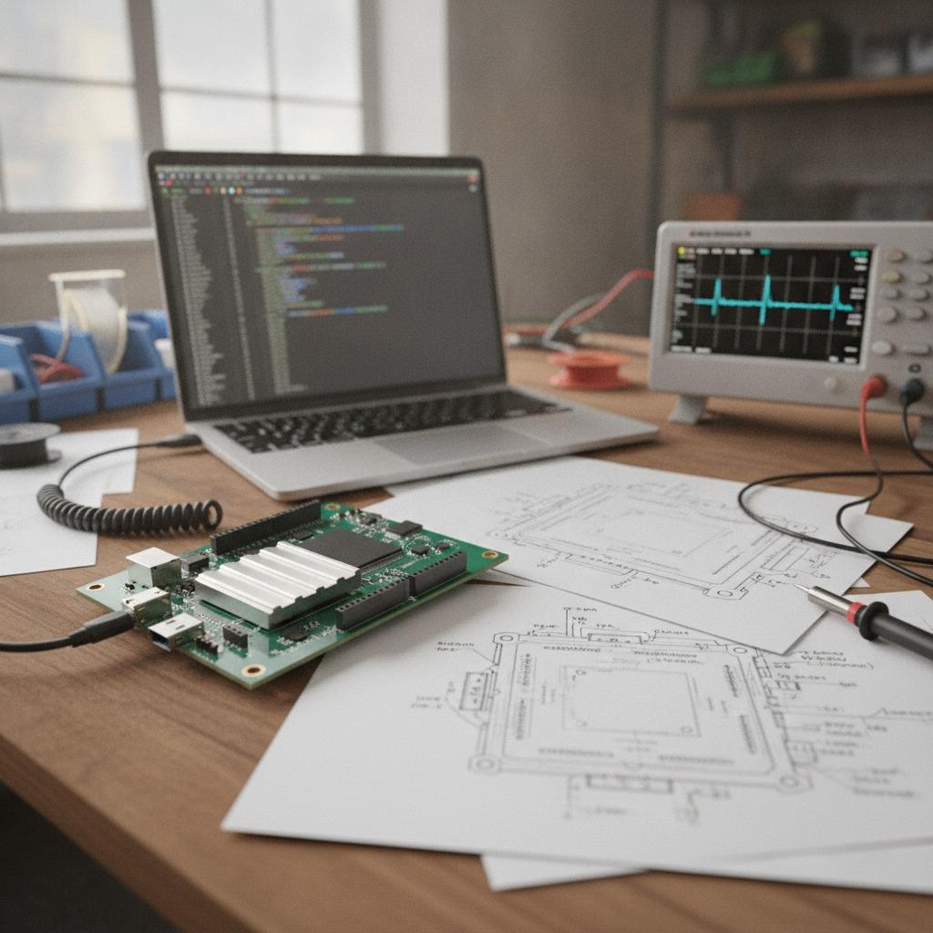
A prototype proves that a concept can be assembled and evaluated; it does not automatically prove that the same design is ready for stable repeat production. Before scaling, an IoT PCBA manufacturer and the buyer should close engineering questions, freeze the approved BOM and PCB revision, define programming and test procedures, resolve fixture requirements, confirm component availability, and establish the approved sample or acceptance reference. The pilot build should then be used to expose production issues that may not appear in a handful of engineering samples. HCDPCBA states that its manufacturing services span prototyping, SMT assembly, sourcing, testing, and OEM/ODM support, and its turnkey PCBA manufacturing guide describes a workflow from engineering review and sourcing through assembly and verification. Project-specific lead time should still be calculated from actual component availability, PCB complexity, quantities, testing preparation, and release status rather than a generic turnaround claim.
Compare IoT PCBA Manufacturing Routes, Not Just Unit Prices
Because many IoT boards are customized, inventing “Model A, Model B, and Model C” simply to create a comparison table would not help a real buyer. A more useful comparison is the manufacturing route being purchased. Before choosing an IoT PCBA manufacturer, confirm whether the quotation covers assembly only, turnkey PCBA, or deeper ODM development, because each route places different engineering, sourcing, testing, and commercial responsibilities on the two parties.
| Project Route | Buyer Normally Provides | Manufacturing Scope to Confirm | Best Fit | Main Cost/Risk Drivers |
|---|---|---|---|---|
| Build-to-print PCBA | Released PCB data, BOM, assembly files and test requirements | PCB/assembly scope, programming, inspection and agreed tests | Mature designs with an established supply chain | Supplied-material shortages, incomplete files, fixture requirements |
| Turnkey IoT PCBA | Released files, approved BOM, quantities and acceptance requirements | PCB, sourcing, SMT/DIP, programming, inspection and testing | OEMs wanting fewer suppliers to manage | BOM availability, approved alternatives, test coverage, procurement lead time |
| ODM + manufacturing | Product requirements, interfaces, application conditions and commercial targets | Engineering development, prototypes, revisions, manufacturing preparation and production | New connected products requiring deeper engineering participation | Development scope, firmware, validation, design ownership and change control |
Understand the Real Cost Drivers in IoT PCBA Manufacturing
The lowest assembly price is rarely meaningful unless every supplier is quoting the same deliverable. IoT PCBA cost can be influenced by PCB size and construction, component count, wireless and processor packages, fine-pitch or BGA assembly, BOM availability, programming, test-fixture development, connectivity verification, coating or special processing when specified, order quantity, and packaging requirements. Procurement teams should separate one-time engineering or tooling costs from recurring unit costs and identify exclusions in each quotation. If one supplier includes component sourcing, firmware loading, functional testing, and documentation while another prices only SMT placement, the two unit prices cannot be compared directly. Cost reduction should therefore start with DFMA, BOM review, panel utilization, approved component alternatives, and test efficiency rather than removing a verification step that the finished IoT product actually needs.
Define OEM and ODM Responsibilities Before Development Starts
For OEM production, the buyer normally has a more defined product specification and expects the manufacturer to reproduce an approved configuration. ODM projects involve greater engineering participation and therefore require more detailed agreement about schematic and PCB design, firmware, prototypes, mechanical interfaces, revision rounds, validation, source-file ownership, tooling, and production transfer. HCDPCBA describes both OEM and ODM within its company services, but the exact scope should be documented for each project. An IoT PCBA manufacturer should not be expected to infer who owns firmware or who is responsible for final wireless certification after development has already started. Defining those responsibilities at the RFQ stage reduces commercial disputes and makes it easier to control changes when the product moves into repeat production.
What Should You Send HCDPCBA for an IoT PCBA Evaluation?
A useful inquiry should include Gerber or approved PCB fabrication data, the BOM with manufacturer part numbers, CPL or pick-and-place data, assembly drawings, schematic where appropriate, firmware or programming requirements, prototype quantity, expected production quantity, application description, wireless requirements, power conditions, mechanical restrictions, test requirements, and target schedule. If the design is not yet frozen, identify what is confirmed and what requires DFMA or ODM support instead of presenting preliminary assumptions as final specifications. Buyers can first review HCDPCBA's PCB and PCBA product range and connected-device examples, then submit project information through the HCDPCBA Contact Us page. The more clearly the initial RFQ defines manufacturing and test responsibilities, the more useful the technical review and quotation can be.
Frequently Asked Questions
1. What files should I send an IoT PCBA manufacturer for quotation?
For a developed design, provide Gerber files, BOM with manufacturer part numbers, placement data, assembly drawings, quantities, and the required inspection and functional-test scope; schematics, firmware, mechanical drawings, and programming instructions are also useful where relevant. If some information remains preliminary, mark it clearly so the quotation can distinguish confirmed scope from assumptions.
2. Can an IoT PCBA manufacturer support Wi-Fi, Bluetooth, Zigbee, or other wireless products?
Wireless support depends on the specific chipset or module, PCB design, firmware, antenna system, and manufacturing requirements. Do not select a manufacturer simply because a webpage lists a protocol; send the actual wireless architecture and determine whether the required assembly, programming, inspection, and verification processes can be supported for that design.
3. How should low-power IoT PCBAs be tested?
Define the operating modes that matter to the final device, including startup, active operation, standby or sleep, wake-up events, sensor activity, and communication behavior where applicable. Establish measurable acceptance limits in the project test specification rather than assuming that a successful power-on check proves low-power performance.
4. How should component substitutions be controlled?
Use an approved BOM with manufacturer part numbers and designate critical parts that require engineering authorization before replacement. For wireless modules, processors, sensors, oscillators, power components, or other function-sensitive parts, evaluate electrical, firmware, mechanical, sourcing, and compliance consequences before approving the alternative.
5. Is AOI enough for an IoT PCBA?
No single inspection method proves every aspect of a connected product. AOI can support visual assembly inspection, while other board features may require different inspection methods and the product may still need electrical, programming, connectivity, or functional verification according to the agreed acceptance plan.
6. Can HCDPCBA support IoT prototypes before mass production?
HCDPCBA describes PCB prototyping, SMT assembly, PCBA manufacturing, DFMA, component sourcing, testing, and OEM/ODM among its services. Prototype quantity, component availability, engineering work, test preparation, and the transition to a pilot or production build should still be evaluated for the specific project.
7. What is the difference between turnkey IoT PCBA and ODM?
Turnkey PCBA typically starts with a substantially defined design and adds sourcing, manufacturing, assembly, and testing coordination. ODM usually involves deeper participation in product development. Because commercial definitions can vary, specify the actual engineering, firmware, testing, tooling, documentation, and manufacturing responsibilities instead of relying only on the label.
8. Can an ESP32 prototype be converted directly into a mass-production IoT PCBA?
A development board can be valuable for firmware, UI, sensor, or connectivity evaluation, but the production design may have different requirements for size, power, interfaces, components, test access, antenna arrangement, and manufacturing cost. HCDPCBA's ESP32-S3 development platform is useful as a prototyping reference, while a custom production board should undergo its own design and manufacturing review.
9. How should certification requirements be handled in an IoT project?
Identify the destination market and required product documentation before production is released. Review which certificates belong to the manufacturing company, which documents apply to individual wireless modules or components, and which approvals remain the responsibility of the finished product. Do not assume one company-level certificate automatically covers every IoT device.
10. What determines IoT PCBA MOQ and lead time?
MOQ and lead time are project-specific because they can depend on PCB fabrication requirements, component purchasing quantities, BOM availability, assembly complexity, programming, test fixtures, verification time, and production volume. Ask the manufacturer to identify these assumptions in the quotation rather than relying on a generic quantity or delivery promise.
Conclusion
Selecting an IoT PCBA manufacturer is ultimately a decision about whether a connected-device design can be transformed into a controlled, testable, and repeatable production process. OEM buyers should define the application first, freeze critical PCB and BOM requirements, control wireless and sensor components, agree on programming and testing responsibilities, verify relevant certification information, and use prototype and pilot stages to remove risk before scaling. HCDPCBA combines PCB prototyping, SMT assembly, DFMA, component sourcing, testing, and OEM/ODM services with IoT-related manufacturing applications described across its website. For a project-specific review, send your design files, BOM, wireless architecture, quantities, test requirements, and production targets through the HCDPCBA contact page so the manufacturing scope can be evaluated against your actual IoT product rather than a generic PCB assembly request.