Why a custom TWS earbud PCBA board is not just another small PCB
A Custom TWS earbud PCBA board sits in a very different category from a generic control board, even if the assembled module looks modest at first glance. In true wireless stereo products, the board has to fit a cramped enclosure, handle battery-related functions, support audio and wireless communication, and survive the realities of mass assembly. That combination makes the PCB assembly decision matter as much as the industrial design.
For engineers and sourcing teams, the real question is rarely “Can this board be built?” It is “Can it be built repeatedly, in a small package, with stable electrical behavior and acceptable test yield?” That is where an OEM wireless earbud pcba solution becomes valuable. It gives product teams a path from concept to a manufacturable subassembly without treating the board as an afterthought.
What buyers should notice first
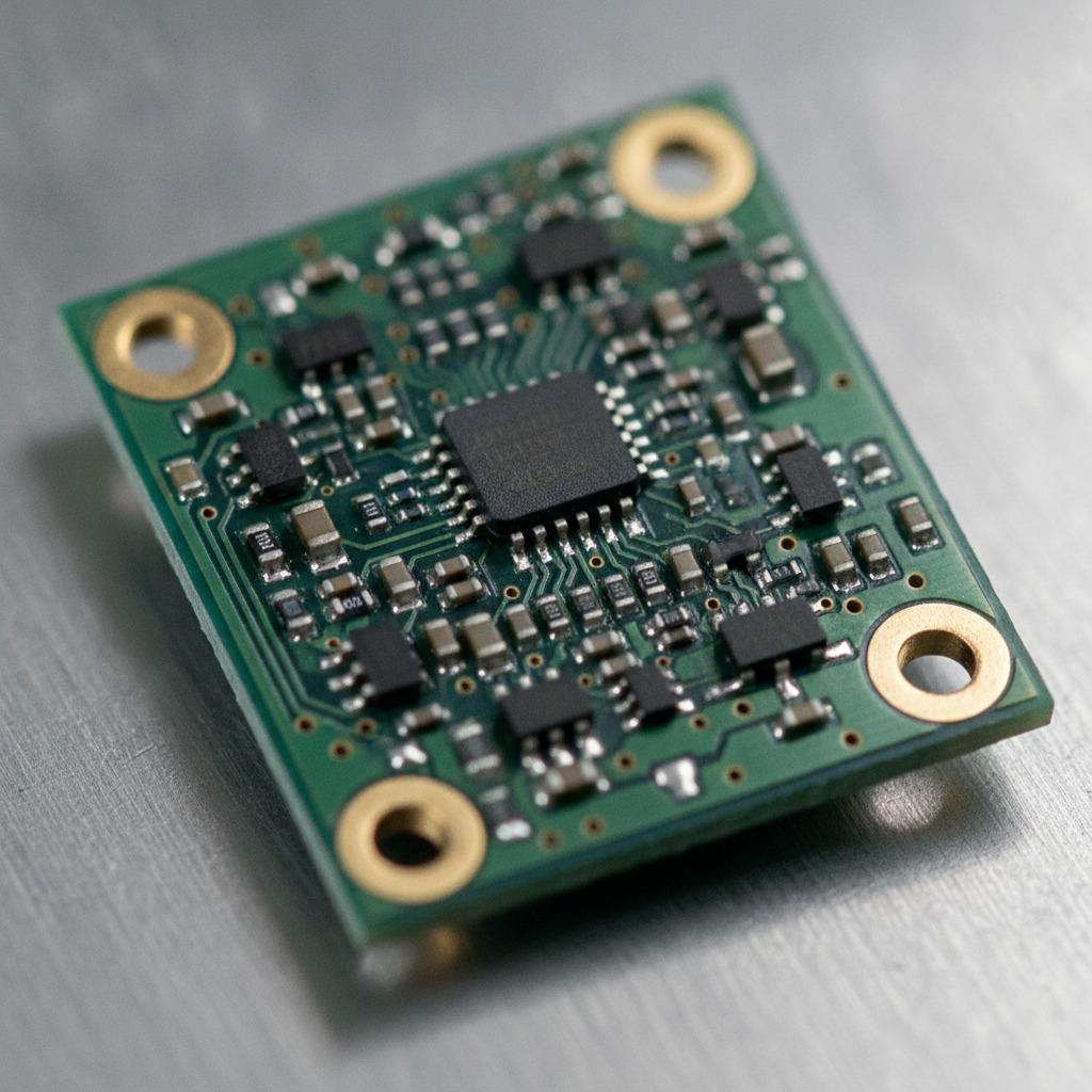
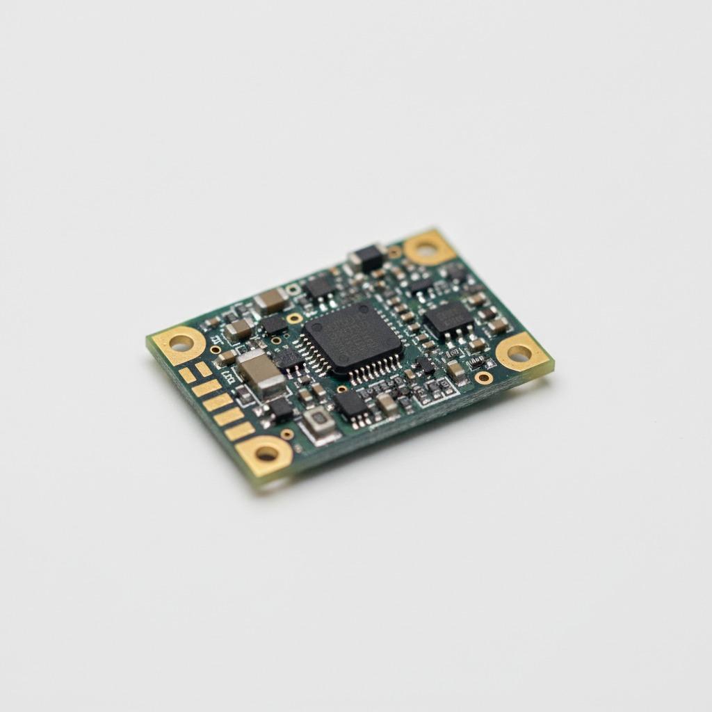
Based on the provided product details, the board class here is a compact PCB assembly with surface-mount components, a central controller or processor package, and mechanical mounting points. Some versions described in the preparation data show gold-plated corner holes, small connector interfaces, and dense component placement. That is typical of a module designed to be dropped into a device enclosure or combined with other subassemblies.
In practical terms, the value is not just in the board itself but in the integration work behind it: PCB fabrication, SMT assembly, soldering, and electrical test. For a TWS earphone PCBA, those steps must be managed with more discipline than in a loose prototype. Small defects that would be tolerable on a lab board can become expensive once the design moves toward pilot production.
Typical build elements in a TWS earbud PCBA
Compact layout and fine-pitch assembly
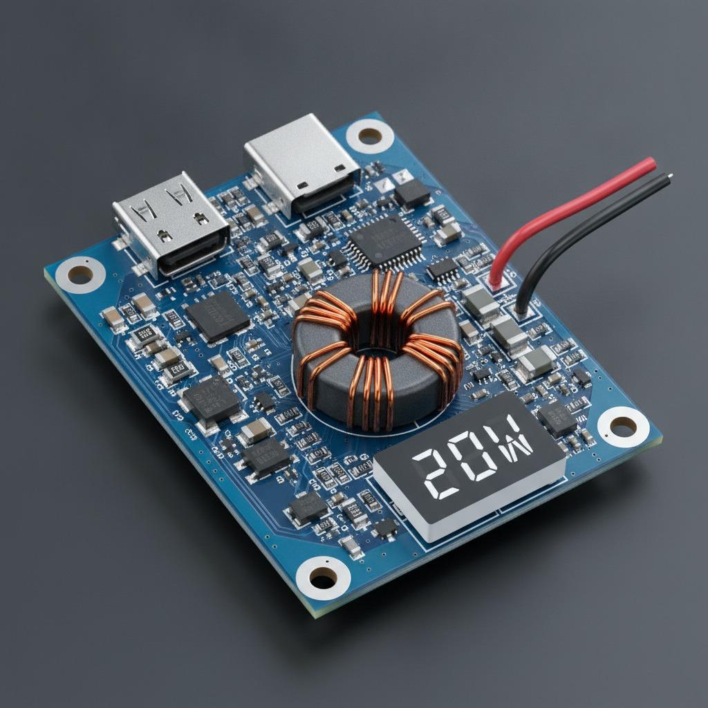
True wireless earbud electronics usually demand dense placement, short signal paths, and careful routing around the main IC. The supplied product information points to FR-4-type construction, green or blue solder mask depending on the sample, and SMT-populated assemblies. That is the normal foundation for a TWS earbud PCBA intended for compact consumer or embedded devices.
Mechanical attachment matters more than it looks
Multiple mounting holes are not decoration. They help secure the board in a shell, reduce movement under vibration, and make repeatable assembly easier. In small audio products, mechanical stability can protect solder joints and keep connector alignment consistent. It is a small feature that often saves trouble later.
Interface choices influence the product architecture
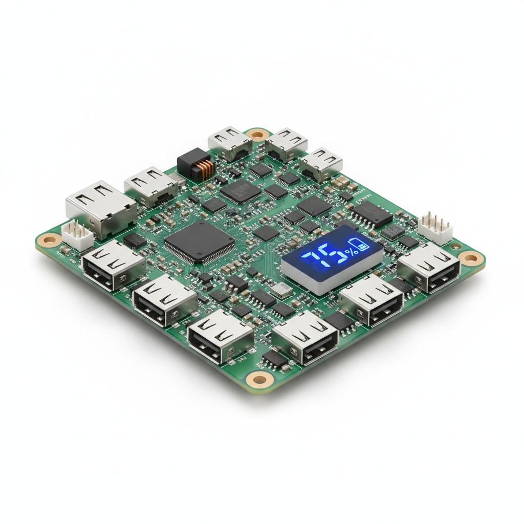
The data mentions edge pads, connectors, and in one variant a micro-USB port plus a JST-style connector. Not every TWS design will use those exact interfaces, but the point stands: the board needs a sane power and interconnect strategy. A board that is difficult to connect, probe, or program can slow factory work and raise the risk of rework.
What an OEM wireless earbud pcba solution should include
A credible OEM wireless earbud pcba solution should go beyond component placement. At minimum, buyers should expect support for PCB fabrication, SMT pick-and-place, reflow soldering, component sourcing, assembly, and functional test. For higher-risk projects, DFMA review is also worth asking for, because tiny layout decisions can affect yield and long-term reliability.
hcdpcba describes a service scope that fits this kind of work: SMT贴片, PCB打样, 元器件代采, 组装, 测试, DFMA服务, plus OEM and ODM support. The practical takeaway is simple. If a supplier can handle both assembly and process feedback, your team gets fewer handoff gaps between design intent and production reality.
Selection criteria that actually help
When comparing suppliers for wireless earbud electronics, do not stop at “can assemble small boards.” Ask how they manage component sourcing, inspection, and test coverage. Ask whether they can support small-batch development first, then scale. Ask how they handle design changes, because TWS programs almost always change after the first samples.
It is also wise to check whether the supplier is comfortable with boards that combine radio, power, and control functions. A Bluetooth earphone PCB assembly is not simply a tiny digital board; it is usually a mixed-signal product with tighter noise and layout expectations than a basic controller module.
Common mistakes in TWS board sourcing
The first mistake is assuming all compact PCBs are interchangeable. They are not. Board thickness, pad design, connector placement, and assembly sequence can all affect fit and function. The second mistake is underestimating test. If a supplier cannot explain how the board is verified after soldering, that is a warning sign.
A third mistake is locking in a design too early. In earbud products, the enclosure, battery, antenna space, and board geometry influence one another. The board may look finished in CAD while still being awkward in production. That is where practical review from an assembly partner earns its keep.
Buyer-facing advice before you place an order
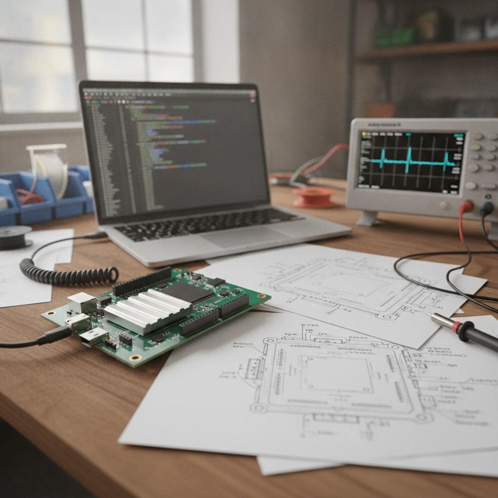
If your team is sourcing a custom earbud board, prepare a complete package: Gerbers, BOM, assembly drawing, test expectations, connector requirements, and any enclosure constraints. If any of those are missing, the risk does not disappear; it simply moves downstream.
For prototype builds, keep the first goal narrow: verify fit, power-up behavior, and basic function. Do not ask a pilot board to prove everything at once unless the test plan is mature. That sounds obvious, but many projects still get trapped by oversized first-pass expectations.
FAQ: short answers that matter
Is a custom TWS earbud PCBA board the same as a finished earbud?
No. It is usually a subassembly inside the product, not the consumer-facing unit.
Can one supplier handle both prototyping and production?
Yes, if they offer PCB prototyping, SMT assembly, sourcing, and test support in one workflow.
Why does compact board layout matter so much?
Because small changes in routing, pad spacing, and mounting can affect assembly yield and final fit.
Next step
If you are developing a wireless earbud platform or another compact embedded product, start with manufacturability, not just circuit function. A supplier such as hcdpcba, with PCB prototyping, SMT assembly, sourcing, testing, and DFMA support, can help move a board from concept to buildable hardware. For sourcing teams, that is often the difference between a clean pilot run and a long round of avoidable rework.
When the board is this small, every decision shows up twice: once in assembly, and again in the field. That is why the right PCBA partner matters.