What Should Buyers Expect From a Smart Home PCBA Project?
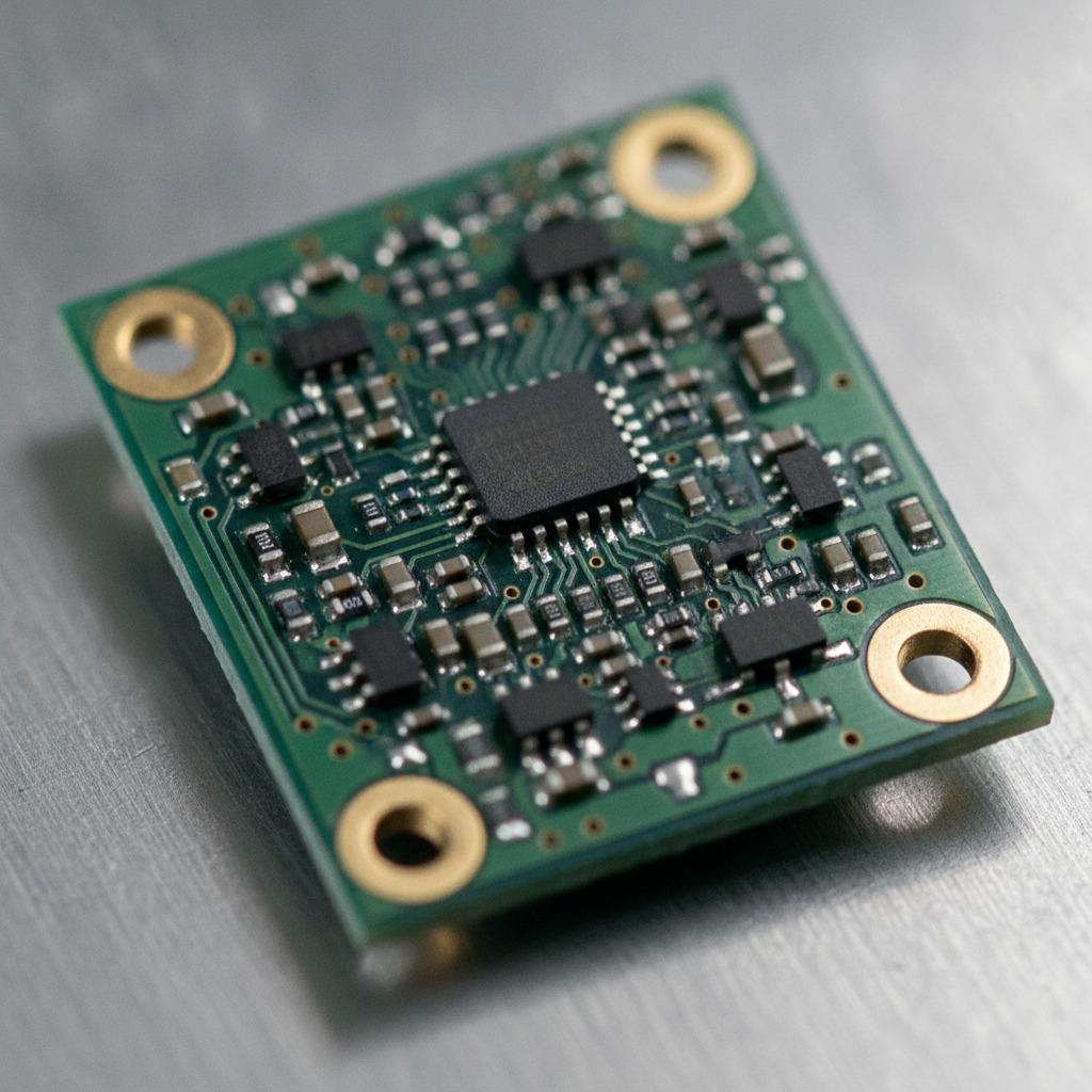
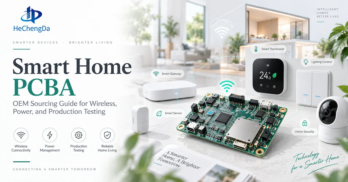
A smart home PCBA is not simply a populated circuit board used inside a connected appliance. In many projects it has to coordinate processing, wireless communication, sensors, power conversion, relays, user interfaces, and firmware while fitting inside a compact enclosure and operating repeatedly in an uncontrolled household environment. For an OEM buyer, the real manufacturing question is therefore not “Can this supplier assemble my PCB?” but “Can this supplier reproduce the approved hardware configuration, program it correctly, verify the functions that matter, and keep that configuration controlled across future orders?” HCDPCBA presents PCB prototyping, SMT assembly, component sourcing, DFMA, assembly/testing, and OEM/ODM support as part of its electronics manufacturing scope, making those capabilities relevant to smart-home development when they are translated into a project-specific production plan. HCDPCBA manufacturing capabilities
Which Buyers Need Custom Smart Home PCB Assembly?
Custom smart-home PCB assembly is most relevant to brands and engineering teams developing smart switches, lighting controls, thermostats, gateways, environmental sensors, security products, access-control devices, connected appliances, energy-management products, and other devices that need electronics matched to a specific enclosure and function. It is also useful when a company has validated an engineering prototype but now needs to convert that prototype into a manufacturable and testable production board. A custom route is less appropriate when an off-the-shelf module already meets the mechanical, electrical, connectivity, documentation, and commercial requirements of the finished product; in that case, adding unnecessary PCB redesign can increase engineering and verification work without creating meaningful product value. HCDPCBA already presents both a Smart Home IoT PCB platform and Smart Home PCB Assembly solutions, which can be used as application references before deciding how much customization a new project actually needs.
Start With the Home Device, Not With the Wireless Protocol
The correct specification begins with what the finished device must do. A wall-mounted smart switch may combine a control MCU, wireless module, relay or switching circuit, status LEDs, buttons or touch inputs, and a power stage; a battery-powered sensor may place much greater emphasis on standby current, wake-up behavior, sensing accuracy, and wireless transmission intervals; a smart-home gateway may need several communication and peripheral interfaces; a security or access-control product may require sensor inputs, audio, imaging, backup power, or other functions. This is why a buyer should not begin a smart home PCBA RFQ with only “Wi-Fi board,” “Bluetooth controller,” or “smart switch PCB.” Define the final product architecture first, then identify which wireless technology, processor, sensors, power scheme, interfaces, and test conditions the PCB assembly must support. HCDPCBA's Wireless Communication PCB application page illustrates the connectivity side of these projects, while the finished RFQ still needs to describe the specific product architecture.
Build a Smart Home PCBA Specification Before Asking for Price
A useful manufacturing quotation starts with a controlled requirement document rather than several disconnected emails. The specification should distinguish information that is already frozen from information that still requires engineering confirmation. That distinction is especially important when purchasing requests an early target price before firmware, wireless architecture, enclosure dimensions, or the BOM has been finalized. The following table is a buyer-side RFQ framework rather than a universal HCDPCBA product specification.
| Requirement Area | What the Buyer Should Define | Why It Matters |
|---|---|---|
| Finished application | Switch, hub, sensor, thermostat, security product, appliance controller or other device | Establishes functional and environmental priorities |
| Power system | Input source, rails, battery or mains-powered architecture, standby and operating modes | Affects circuit, components, heat and testing |
| Wireless architecture | Selected module/chipset, antenna method and required communication functions | Influences layout, sourcing, firmware and verification |
| Processor and memory | Approved MCU/processor, memory and programming requirements | Controls sourcing and firmware configuration |
| Sensors and interfaces | Sensor types, GPIO, UART, I²C, SPI, USB or other required interfaces | Defines integration and functional-test coverage |
| Output/control loads | Relays, LEDs, motors, buzzers or other controlled devices | Determines output-stage requirements and load testing |
| PCB requirements | Board dimensions, layer structure, material, copper, finish and controlled requirements | Defines fabrication scope |
| Mechanical limits | Mounting holes, connector positions, antenna clearance and height restrictions | Determines enclosure compatibility |
| Firmware | Approved revision, programming method and device-specific information | Requires controlled production programming |
| Testing | Power, interfaces, connectivity, sensors, outputs and other acceptance criteria | Determines fixture and shipment-release requirements |
| Production control | Revision marking, traceability, labels, packaging and change approval | Protects repeat-order consistency |
Control Wireless Modules, Sensors, Relays, and Power Components
Component control is one of the most important parts of a commercial smart home PCBA program because a substitution can affect more than purchasing cost. Changing a wireless module can affect layout, firmware, antenna behavior, enclosure integration, and product documentation; changing a sensor can alter measurement behavior or calibration; changing a relay may affect electrical ratings, mechanical dimensions, or switching behavior; changing a regulator can influence efficiency, heat, standby consumption, and EMC behavior. A production BOM should therefore include approved manufacturer part numbers and clearly identify which components require engineering authorization before substitution. Where approved alternatives are necessary for supply-chain resilience, qualify them before an urgent shortage occurs rather than allowing the first evaluation to take place during a delayed production order. HCDPCBA's broader IoT PCB assembly services include component sourcing as part of connected-device manufacturing, but the actual substitution authority and approved-source rules should be defined in the individual project.
DFMA Must Consider Wireless, Power, Test Access, and Enclosure Integration Together
Design for manufacture and assembly should be completed before a pilot build becomes a volume-production problem. A useful review checks footprints, polarity, connector orientation, component spacing, panelization, solderability, component-height restrictions, programming access, test points, mounting features, and any areas where the PCB interacts with the enclosure. Wireless products add another concern: antenna location and nearby components or mechanical structures should remain consistent with the approved design so production changes do not inadvertently alter the finished hardware configuration. Where a smart-home device switches higher voltages or loads, electrical separation and product-safety requirements must also be defined according to the applicable design and destination-market requirements rather than guessed by the assembly factory. HCDPCBA lists DFMA alongside its PCB and PCBA manufacturing services; buyers should use that review to resolve manufacturing questions while retaining engineering approval over circuit function and safety requirements. Learn about HCDPCBA's PCBA services
Production Testing Should Reproduce Important Device Functions
An assembled board powering on is not enough evidence that a smart-home product is ready for shipment. The production test strategy should be linked to the functions that can realistically fail because of assembly, programming, component, or configuration problems. Depending on the product, this may include verifying power rails, firmware programming, wireless-module communication, sensor response, buttons or touch inputs, LEDs, relays, interfaces, and other outputs. Inspection and functional verification should also be separated conceptually: AOI can identify visible assembly issues, X-Ray can be useful for selected hidden solder connections, and functional testing addresses whether the programmed assembly performs the agreed behaviors. HCDPCBA states that AOI and X-Ray are part of its quality-control resources, but a buyer should still document which inspection and test stages apply to the actual smart home PCBA, what the pass/fail criteria are, and whether a fixture or reference sample is required. HCDPCBA quality and manufacturing overview
Wireless Production Checks Are Not the Same as Final RF Validation
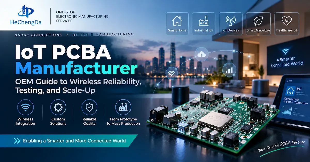
A production line can verify that a wireless module is correctly assembled, programmed, and able to communicate without proving every aspect of final wireless performance. Product-level behavior may also depend on antenna design, enclosure material, battery or power circuitry, nearby metal, firmware, installation location, and interference from other devices in the home. Buyers should therefore define two different objectives: production checks that identify assembly or configuration errors, and product validation that confirms the complete device meets its intended connectivity requirements. This distinction becomes increasingly important when a single smart home PCBA is expected to support several product variants or enclosure configurations. For a broader discussion of wireless, BOM, test, and scale-up issues in connected devices, HCDPCBA's IoT PCBA Manufacturer Guide provides a complementary manufacturing perspective.
Separate Factory Quality Systems From Finished-Product Compliance
Supplier qualification and product compliance are related but different. A manufacturing site can maintain company-level quality or environmental systems, while the finished smart-home device may have separate electrical, wireless, environmental, labeling, or market-access requirements depending on the product and destination country. Buyers should therefore request the documents relevant to the manufacturing company and separately determine what evidence is needed for their finished device. If a wireless module, power architecture, enclosure, controlled component, or other significant element changes, the responsible compliance team should determine whether existing product documentation remains applicable. The safest procurement approach is to define documentation responsibilities during development rather than asking about certifications only after production samples have been completed.
Move From Prototype to Pilot Production Before Scaling
Prototype success proves that a design can work; it does not automatically demonstrate that the same configuration can be reproduced economically and consistently in repeated production. Before scaling, the buyer and manufacturer should close open DFMA items, freeze the PCB revision and approved BOM, control firmware, establish programming instructions, define inspection and functional tests, confirm fixture requirements, and agree on the reference sample or acceptance criteria. A pilot build can then expose problems involving assembly sequence, test time, material handling, programming, fixture access, or mechanical fit before they affect a larger order. HCDPCBA's Turnkey PCBA Manufacturing Guide describes PCB fabrication, sourcing, assembly, testing, and engineering support as interconnected production stages, which is the right framework for assessing a smart-home project rather than treating SMT placement as the complete manufacturing process.
Do Not Compare Smart Home PCBA Quotes Until the Scope Is Equal
There is no useful “standard price” for custom smart-home electronics without defining what each quotation includes. One supplier may quote customer-supplied material assembly, another may include PCB fabrication and component purchasing, and a third may include programming, fixtures, functional testing, packaging, and engineering support. Instead of inventing model comparisons for a customized product, buyers can compare the three common project routes below.
| Project Route | Buyer Normally Provides | Supplier Scope to Confirm | Best Fit | Main Purchasing Risk |
|---|---|---|---|---|
| Build-to-print assembly | Released PCB, BOM, placement files, materials or sourcing instructions, test requirements | SMT/THT assembly, programming, inspection and agreed testing | Mature design with established engineering control | Missing files, supplied-material issues and unclear test scope |
| Turnkey smart home PCBA | Released design, approved BOM, quantities and acceptance requirements | PCB, component sourcing, assembly, programming, inspection and testing | OEM wanting one manufacturing partner | Component substitutions, sourcing lead time and quotation exclusions |
| ODM development + production | Product concept, application requirements, interfaces, enclosure limits and commercial targets | Engineering, prototypes, design revisions, manufacturing preparation and production | New or substantially customized products | Undefined ownership, engineering scope and validation responsibility |
What Actually Drives Smart Home PCBA Cost?
Unit assembly cost is only one part of the commercial decision. PCB construction, board size, component density, wireless and processor packages, sourcing conditions, relay or power stages, programming, test-fixture development, functional-test time, expected quantity, packaging, and engineering changes can all affect project cost. A quotation that includes BOM purchasing, programming, functional verification, and production records cannot be compared directly with one that covers only SMT placement. Procurement teams should first normalize the manufacturing scope, then evaluate cost-reduction opportunities through DFMA, panel utilization, approved alternatives, test efficiency, or design simplification. Removing required test coverage simply to achieve a unit-price target can transfer cost from manufacturing into field failures, returns, troubleshooting, or warranty handling.
Define OEM and ODM Responsibilities Before the First Prototype
OEM and ODM are useful commercial labels, but they are not detailed statements of responsibility. For a build-to-print OEM project, determine who controls schematics, PCB files, firmware, BOM approval, functional specifications, and engineering changes. For an ODM project, additionally define who develops the circuit, selects key components, writes or modifies firmware, prepares prototypes, supports compliance activities, owns resulting design files, and approves the final production configuration. Confidentiality, source-file access, tooling ownership, fixture ownership, and later engineering-change costs should also be settled before substantial development begins. HCDPCBA describes both OEM and ODM support in its manufacturing offering; the buyer should convert that general capability into a written project scope rather than relying on the abbreviation alone. Review HCDPCBA's OEM/ODM manufacturing scope
What Should You Send HCDPCBA for a Smart Home PCBA RFQ?
For an existing design, prepare Gerber and drill data, BOM with manufacturer part numbers, pick-and-place data, assembly drawings, board dimensions, schematics where appropriate, firmware or programming files, prototype and production quantities, mechanical restrictions, connectivity requirements, test requirements, and the target schedule. For a new development project, add the intended device application, power source, wireless architecture, sensors and controlled loads, enclosure information, required interfaces, destination market, and unresolved engineering questions. Buyers can review HCDPCBA's PCB and PCBA product range and its Smart Home IoT PCB application example before submitting a project. When the technical package is ready, use the HCDPCBA Contact Us page to request a manufacturing review based on the actual board and acceptance requirements rather than only a target unit price.
Frequently Asked Questions
1. What is a smart home PCBA?
A smart home PCBA is an assembled printed circuit board used to provide control, sensing, communication, power-management, user-interface, or output functions inside a connected home device. The exact architecture varies by application, so the manufacturing requirements for a sensor, switch, gateway, security product, and connected appliance should not be assumed to be identical.
2. What files are needed for a smart home PCB assembly quotation?
For a mature design, buyers should normally prepare PCB fabrication data, BOM, placement data, assembly information, quantities, and test requirements. Schematics, mechanical drawings, firmware, programming instructions, and an application description can help resolve engineering questions that cannot be answered from Gerber files alone.
3. Can the same PCBA be used for Wi-Fi, Bluetooth, Zigbee, Thread, or other wireless products?
That depends on the selected wireless architecture, module or chipset, firmware, antenna arrangement, board layout, and product requirements. A buyer should define the required protocol and hardware rather than assume that a generic IoT PCB can support every connectivity method without modification.
4. How should a smart switch PCB assembly be evaluated?
Start with the supply architecture, controlled load, switching component, wireless system, manual controls, enclosure, thermal conditions, and required product-safety criteria. Then define production tests that verify the functions relevant to the approved design rather than relying only on visual inspection.
5. Is AOI enough for smart-home electronics?
AOI is useful for detecting selected visible assembly defects, but it does not prove firmware, wireless communication, sensor operation, relay switching, power behavior, or every hidden solder connection. The production plan should combine appropriate inspection methods with electrical or functional verification based on the device architecture.
6. How should wireless-module substitutions be handled?
A wireless-module change should go through engineering review because it can affect electrical interfaces, firmware, antenna behavior, sourcing, mechanical integration, and documentation. Record approved alternatives in the controlled BOM rather than allowing purchasing substitutions to be made informally.
7. What is the difference between turnkey smart home PCBA and ODM?
Turnkey manufacturing generally begins with a substantially completed customer design and adds PCB fabrication, sourcing, assembly, programming, inspection, and testing according to the agreed scope. ODM involves more development responsibility, so design ownership, firmware, prototypes, validation, and engineering-change responsibilities must be defined separately.
8. How is smart home PCBA lead time determined?
Lead time depends on the board design, PCB fabrication requirements, component availability, purchasing quantities, assembly complexity, programming, test fixtures, verification scope, production volume, and whether the design is fully released. Buyers should request a project-specific schedule with its starting conditions instead of relying on a generic turnaround statement.
9. How can OEM buyers reduce smart home PCB assembly cost?
First compare quotations with the same scope. Then review PCB panelization, BOM availability, approved component alternatives, manufacturing complexity, fixture reuse, programming efficiency, and test cycle time with the engineering team. Cost reduction should preserve the functions and verification necessary to release the finished product.
10. How can repeat-order consistency be protected?
Control the approved PCB revision, BOM, firmware, programming process, assembly instructions, test limits, labels, packaging, and authorized alternatives. Require documented review before changing any of these elements so future production remains tied to the same approved product definition.
Conclusion
A successful smart home PCBA program depends on much more than accurate component placement. Smart-home brands and OEM buyers need to define the device application, wireless and power architecture, approved components, mechanical constraints, firmware, testing, compliance responsibilities, and change-control process before expecting stable repeat production. The most useful manufacturing partner is therefore one that can translate released engineering information into a controlled production process and clearly identify what still requires buyer approval. HCDPCBA combines PCB prototyping, component sourcing, SMT/PCBA manufacturing, DFMA, testing, and OEM/ODM support with smart-home and IoT application experience described across its website. For a project-specific review, submit your design files, BOM, device application, wireless architecture, quantities, programming needs, and testing requirements through the HCDPCBA Contact Us page so the manufacturing proposal can be built around your actual smart-home product rather than a generic PCB assembly request.