Single-Chip DAC Development Board Overview
The Single-Chip DAC Development Board is built for engineers who need a compact way to turn digital signals into usable analog output without spending time on a full custom board first. It helps solve a common development problem: how to quickly evaluate a conversion circuit, bring signals out to headers, and integrate the module into a larger prototype or control system. Based on the visible board structure, this type of module is well suited for embedded testing, interface work, and early-stage hardware validation.
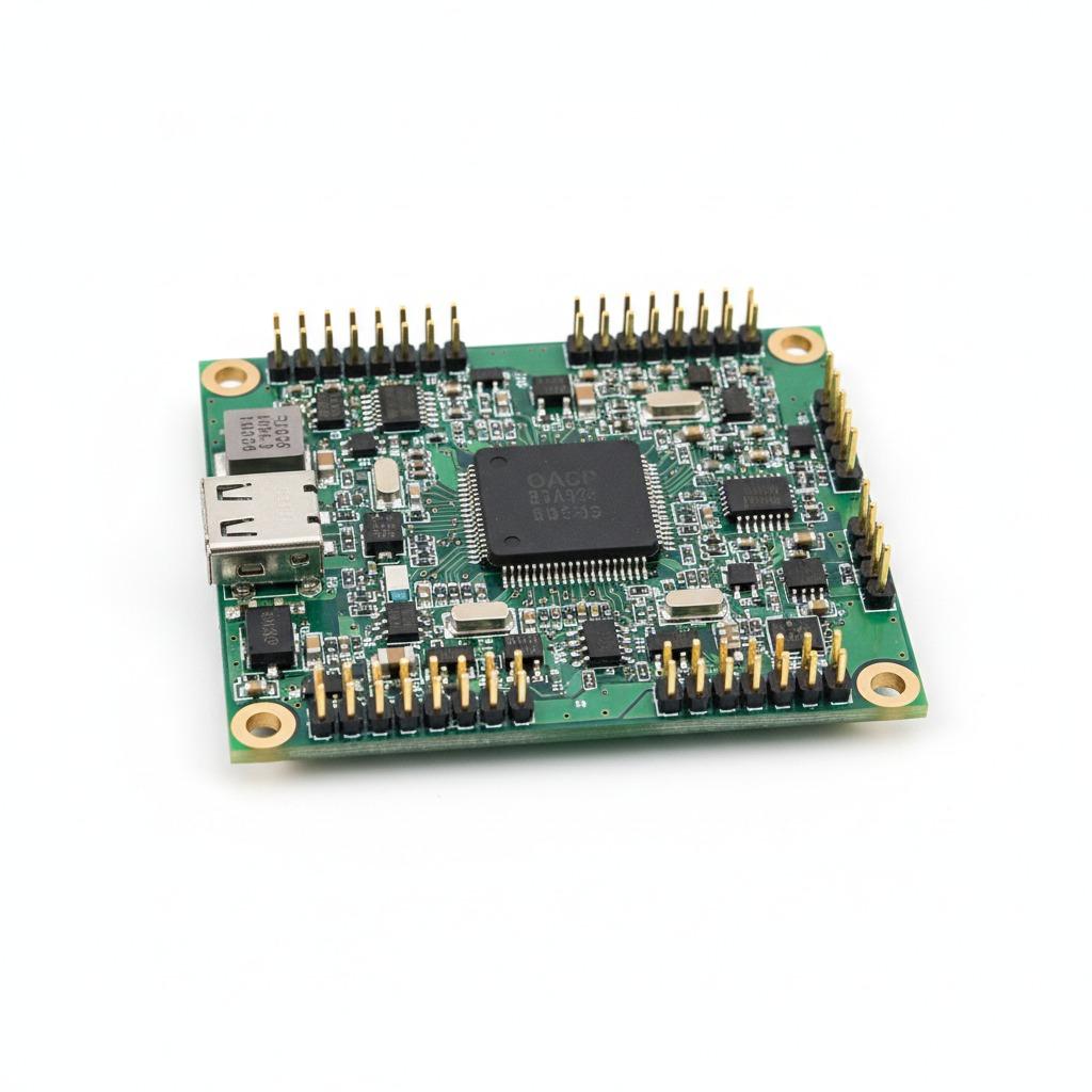
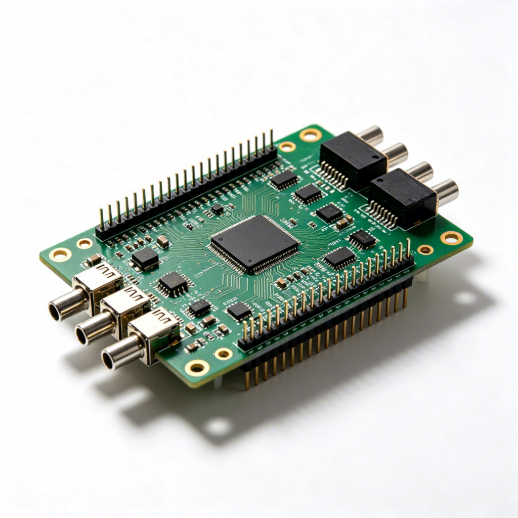
From the image, the board appears to be a populated PCB assembly with a central square IC, rows of gold-plated pin headers, mounting holes, and supporting components around the signal path. That layout suggests a practical development platform rather than a bare layout. It is also the sort of board that can be adapted into a wider range of OEM or lab setups, especially when buyers need a single chip digital to analog conversion module that can be mounted, wired, and tested quickly.
Product Structure and Visible Features
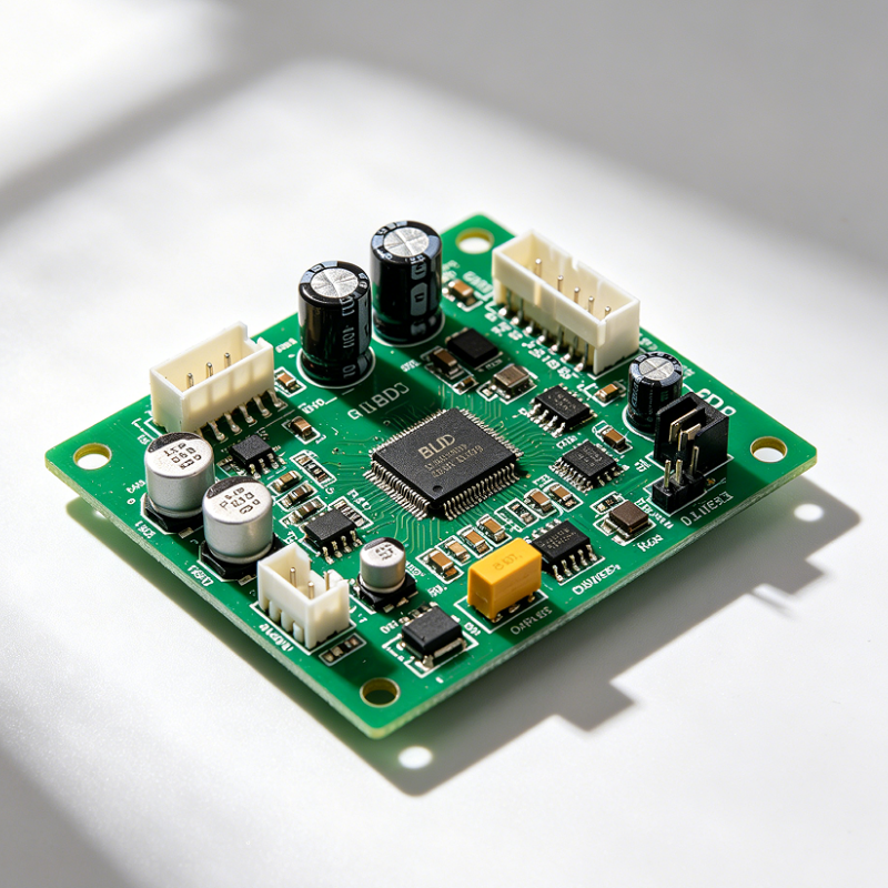
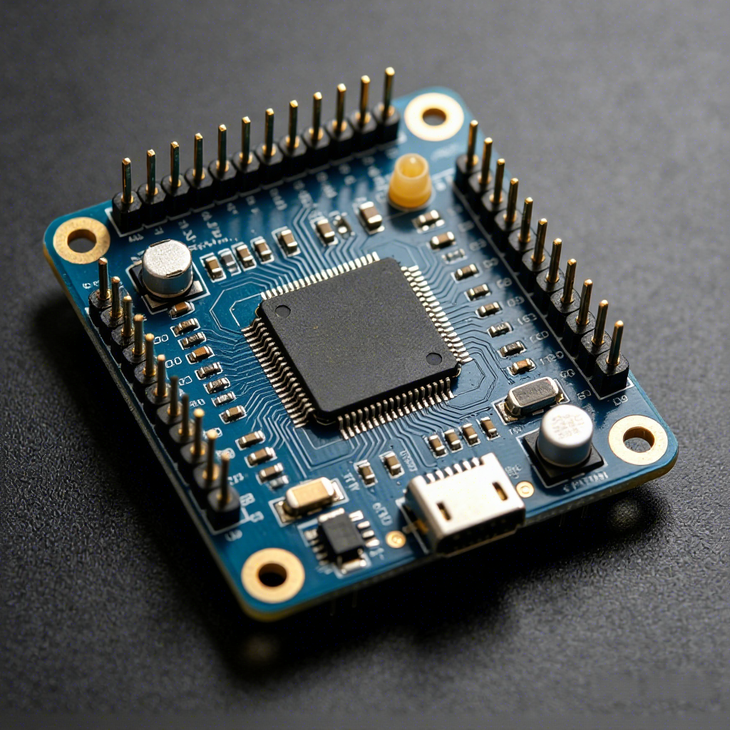
The board uses a compact rectangular format with a blue solder mask, white silkscreen, and FR-4-style construction. Several visible features stand out immediately: a central fine-pitch IC package, small passive components placed close to the main device, a metal-shielded can or connector area, and a micro-USB port on one version of the board image. These details indicate a design intended for signal handling and board-level integration.
What is clearly visible
There are multiple rows of through-hole pin headers around the edges, which makes the board easy to connect during prototyping. The plated mounting holes improve mechanical stability when the board is fixed inside a test fixture or enclosure. A shielded metal component area suggests the designer has considered EMI-sensitive sections or protected connectivity. A buyer looking for a Digital to Analog Converter with Pin Header & Jumper will likely value this kind of straightforward physical interface.
Key Capabilities for Development and Integration
Because the exact chip model and firmware are not identifiable from the image alone, it is best to treat this module as a hardware platform for signal conversion, control, or interfacing rather than assuming a specific protocol or output range. What can be confirmed is the board’s suitability for compact electronic systems that need a small footprint and accessible I/O.
Typical strengths in use
The header layout supports direct connection to controllers, external sensors, actuators, or test equipment. The dense central IC package points to a more integrated design, which is common in boards built for control logic or analog output generation. For engineers comparing evaluation hardware, a Pin header DA conversion development board can reduce setup time because the connection points are already exposed and labeled on the PCB.
Materials and Finish Options
The visible boards show standard electronics manufacturing materials: fiberglass-reinforced PCB substrate, solder mask finish, gold-colored header pins, and black plastic header housings. These are common choices for reliable board assembly because they balance solderability, electrical performance, and mechanical strength.
Although the supplied image does not confirm alternative builds, similar boards can often be produced with different solder mask colors, surface finishes, or connector arrangements depending on project needs. For teams requesting Professional PCB & PCBA Services, the most important decision is usually not color, but how well the board stack, assembly method, and connector placement match the final enclosure and test workflow.
Manufacturing Process
This type of product normally combines PCB fabrication with SMT assembly and through-hole soldering. The central IC and surrounding passives are mounted by surface-mount processes, while the pin headers and any connectors are installed through holes for stronger mechanical retention. That mix is common in development modules because it supports both circuit density and easy external wiring.
hcdpcba offers PCB fabrication, SMT placement, component sourcing, assembly, and testing services. For a board like this, DFMA review can be especially useful early in the project. It helps confirm whether the connector spacing, component placement, and assembly sequence are practical before pilot production starts.
Application Scenarios
This module form factor fits a wide range of electronics work. It can be used in embedded prototyping, robotics, automation benches, industrial controller integration, lab fixtures, sensor interface boards, or compact evaluation setups. The exact use depends on the hidden circuit function, but the physical design clearly supports repeated connection and disconnection during development.
In OEM and ODM projects, boards like this often serve as a bridge between concept and final product. They allow teams to validate signal routing, connector access, and assembly methods before committing to a custom housing or a larger multilayer design.
Quality Control and Buyer Decision Factors
When choosing a board of this type, buyers should look closely at a few practical points: header alignment, solder joint quality, mounting hole consistency, silkscreen readability, and connector placement. If the module will be installed into a larger system, mechanical fit matters as much as circuit behavior.
Quality control for PCBA usually includes visual inspection, assembly verification, and electrical testing where applicable. Since the exact electrical performance is not shown in the image, buyers should request pinout documentation, test criteria, and assembly notes before scaling production. That is especially important when the board is intended for industrial, communications, or mixed-signal work.
Customization Guidance
If your project needs a different connector layout, board outline, or component sourcing strategy, the design can usually be adapted during the PCB and PCBA stage. A custom version may include repositioned headers, alternate mounting holes, or integration with a specific enclosure. For teams building a new module, it is smart to define the electrical interface first and then align the mechanical design around it.
hcdpcba supports small-batch and volume manufacturing, including OEM and ODM workflows. That makes it easier to move from prototype boards to repeatable production while keeping assembly and testing under one process flow.
Contact for PCB Assembly Support
If you are developing a board around a single conversion IC, or you need a reliable PCB assembly partner for a compact control module, hcdpcba can help with PCB prototyping, SMT assembly, component procurement, and testing. Share your drawings, BOM, and interface requirements, and the team can review manufacturability before production begins.
For project discussion or quotation requests, contact hcdpcba at +86 18924624188.