Matter Protocol PCBA Overview
Matter Protocol PCBA is designed for projects that need a compact control and communication board for connected devices. For buyers building smart products, the main challenge is often not just fitting electronics into a small enclosure, but also keeping interfaces organized, stable, and easy to assemble. A Matter Protocol PCBA supports that need by combining PCB fabrication, SMT assembly, and connector integration into one practical module for embedded control, prototyping, or OEM system design.
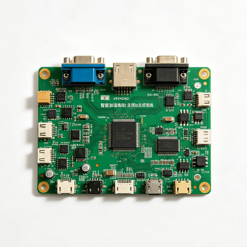
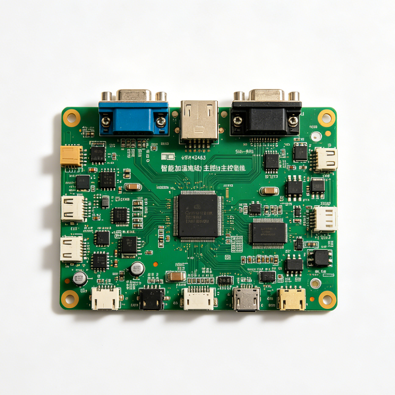
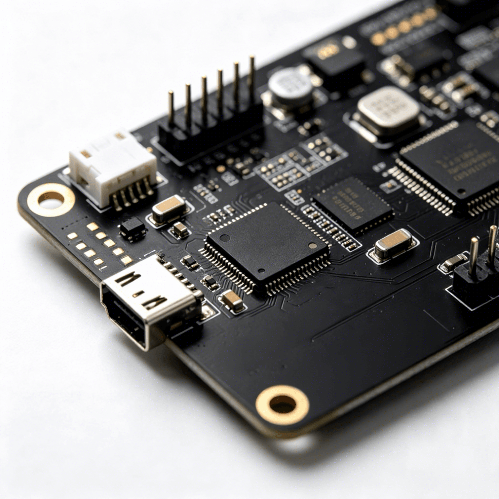
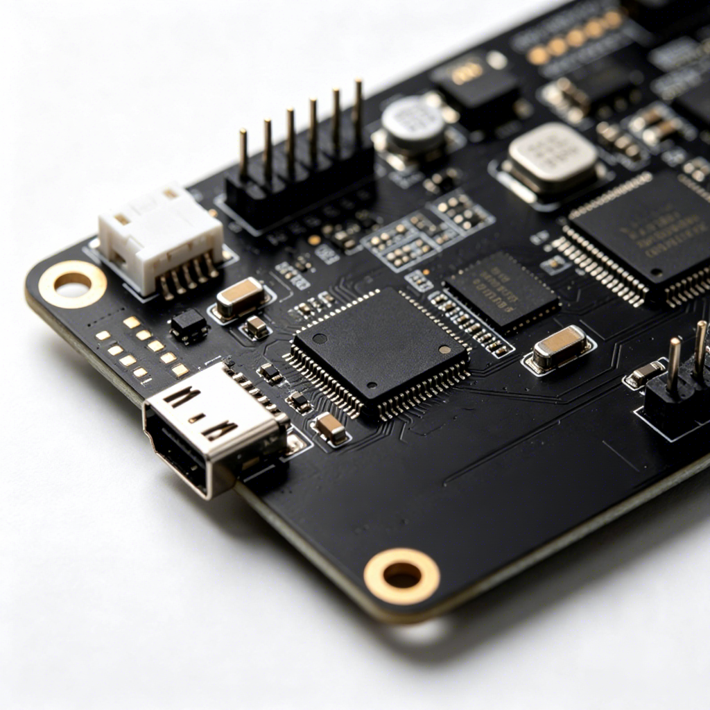
From the visible structure, this type of board is suitable for electronics development where multiple external connections, board mounting, and signal handling are required. The board shows a dense component layout, corner mounting holes, and a mix of surface-mounted and through-hole parts, which is typical for a compact electronic assembly used in interface or control applications.

Product Structure and Visible Features
This board appears to use a compact square format with rounded corners and four mounting holes for mechanical fastening. The substrate is a dark-colored PCB with a matte solder mask, while the mounting holes show copper or gold-plated rings that help with durability and grounding contact. The assembly includes a central IC, smaller support chips, passive components, headers, and at least one USB Type-A female connector. Some versions visible in the supplied data also show dual USB ports, which suggests the board can support multiple connection points.
Because the exact model and function are not identifiable from the image alone, it is safest to describe the board as an embedded electronics module or controller-style PCBA rather than a finished consumer product. That makes it relevant for integration into larger systems, development platforms, or custom hardware builds.
Key Capabilities and Practical Use
Connection and interface support
The visible USB connector and edge headers indicate the board is intended to communicate with external devices, test equipment, or host systems. Multiple connector options are useful when a design must interface with sensors, actuators, expansion modules, or debugging tools.
Compact embedded layout
A dense PCB layout helps reduce overall footprint, which matters in smart devices and industrial electronics where enclosure space is limited. The arrangement of ICs and passives suggests the board is built for signal processing, device control, or communication tasks.
Mechanical integration
Four mounting holes make it easier to secure the board inside a housing or fixture. This is important for vibration control, assembly consistency, and serviceability in production environments.
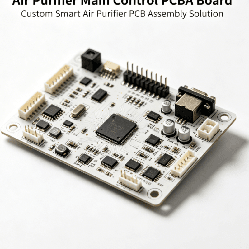
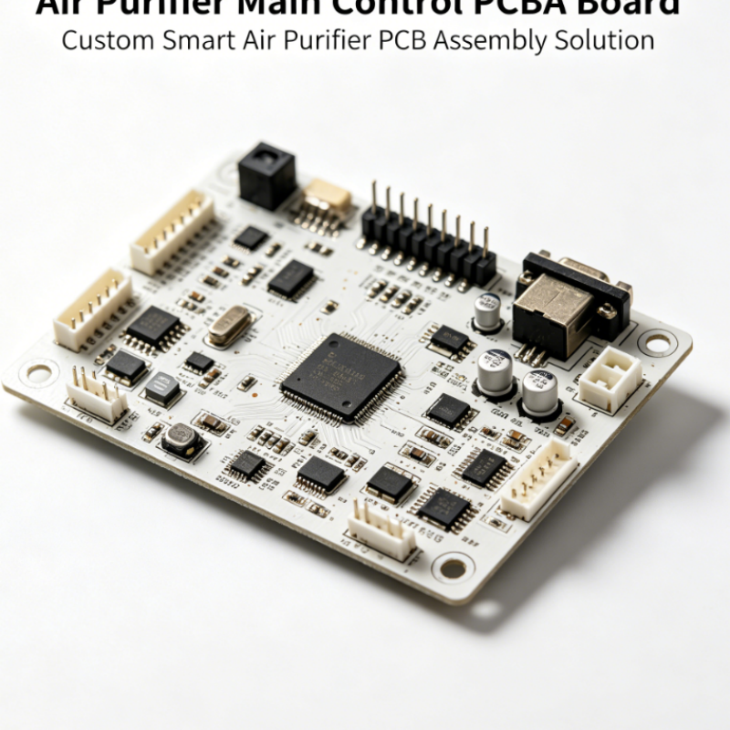
Materials and Finish Options
The visible board uses a standard FR-4 style construction with copper traces and solder mask. The black or dark finish gives a clean look and helps highlight the component placement. For related builds, customers may request different solder mask colors, silkscreen layouts, pad finishes, connector styles, or protective coatings depending on the application.
In a PCBA project, finish selection often depends on assembly requirements, environmental exposure, and inspection needs. If the board will be used in a smart home product or industrial controller, finish choices should be matched to the electrical and mechanical design rather than appearance alone.
Manufacturing Process
This kind of board is typically produced through PCB fabrication followed by SMT assembly and selective through-hole insertion for headers or connectors. The process may include solder paste printing, pick-and-place placement, reflow soldering, through-hole soldering, inspection, and functional testing. For a Matter Protocol PCBA, assembly quality is especially important because signal integrity and connector reliability affect system stability.
hcdpcba supports PCB prototype work, SMT assembly, component sourcing, testing, DFMA review, and OEM or ODM service. That makes it suitable for buyers who need both manufacturing support and engineering coordination during product development.
Application Scenarios
This board format can be used in embedded systems development, industrial control interfaces, sensor and actuator integration, data acquisition modules, test fixtures, and USB-connected electronics. It also fits well in smart device projects where a compact controller board must communicate with other modules inside a final product.
Related search terms such as Smart Home PCBA and Intelligent Home Circuit Board are often used for boards like this when they are integrated into connected appliances, home automation devices, or control hubs. However, the exact end use should always be confirmed by the customer specification, since the visible board alone does not reveal the full firmware or protocol stack.
Quality Control and Buyer Decision Factors
When sourcing this type of PCBA, buyers should focus on component placement accuracy, solder joint consistency, connector alignment, mounting-hole precision, and test coverage. It is also important to confirm the BOM, interface pinout, voltage requirements, firmware needs, and inspection standard before production begins.
For custom projects, the most important decision factors are board size, connector count, assembly method, test strategy, and whether the design will move from prototype to volume production. A good supplier should be able to support sample builds, process review, and changes during iteration without disrupting the overall schedule.
Customization and OEM Support
Customization can include connector placement, board outline changes, silkscreen updates, component substitution, assembly optimization, and production test planning. If the design is intended for a Smart Home PCBA or another intelligent control platform, customization should also consider enclosure fit, cable routing, and downstream integration.
hcdpcba provides SMT, PCB prototype support, component procurement, assembly, testing, and OEM/ODM services for customers who need a reliable electronics manufacturing partner. If you are developing a compact controller board or refining an embedded module for your product line, send your Gerber files, BOM, and assembly requirements for evaluation and quotation.