Why WiFi and Bluetooth boards are harder than they look
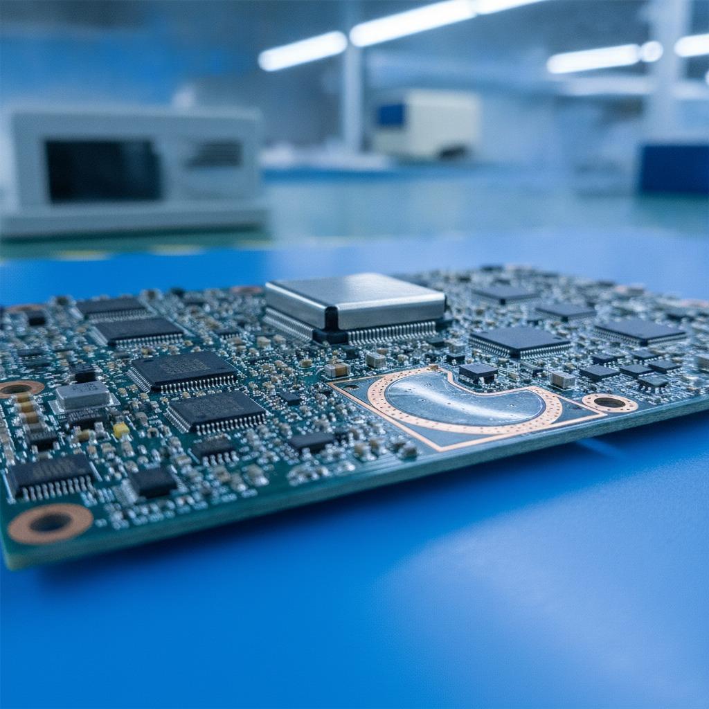
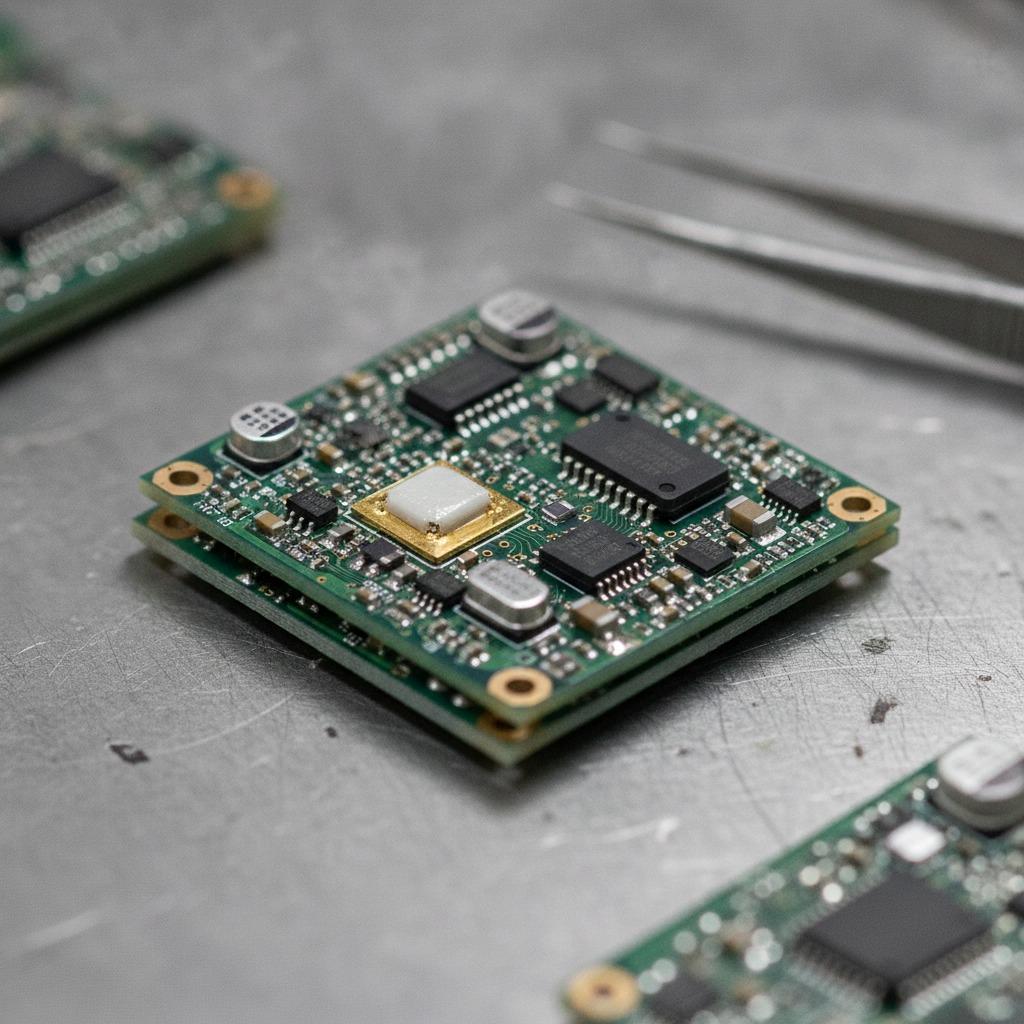
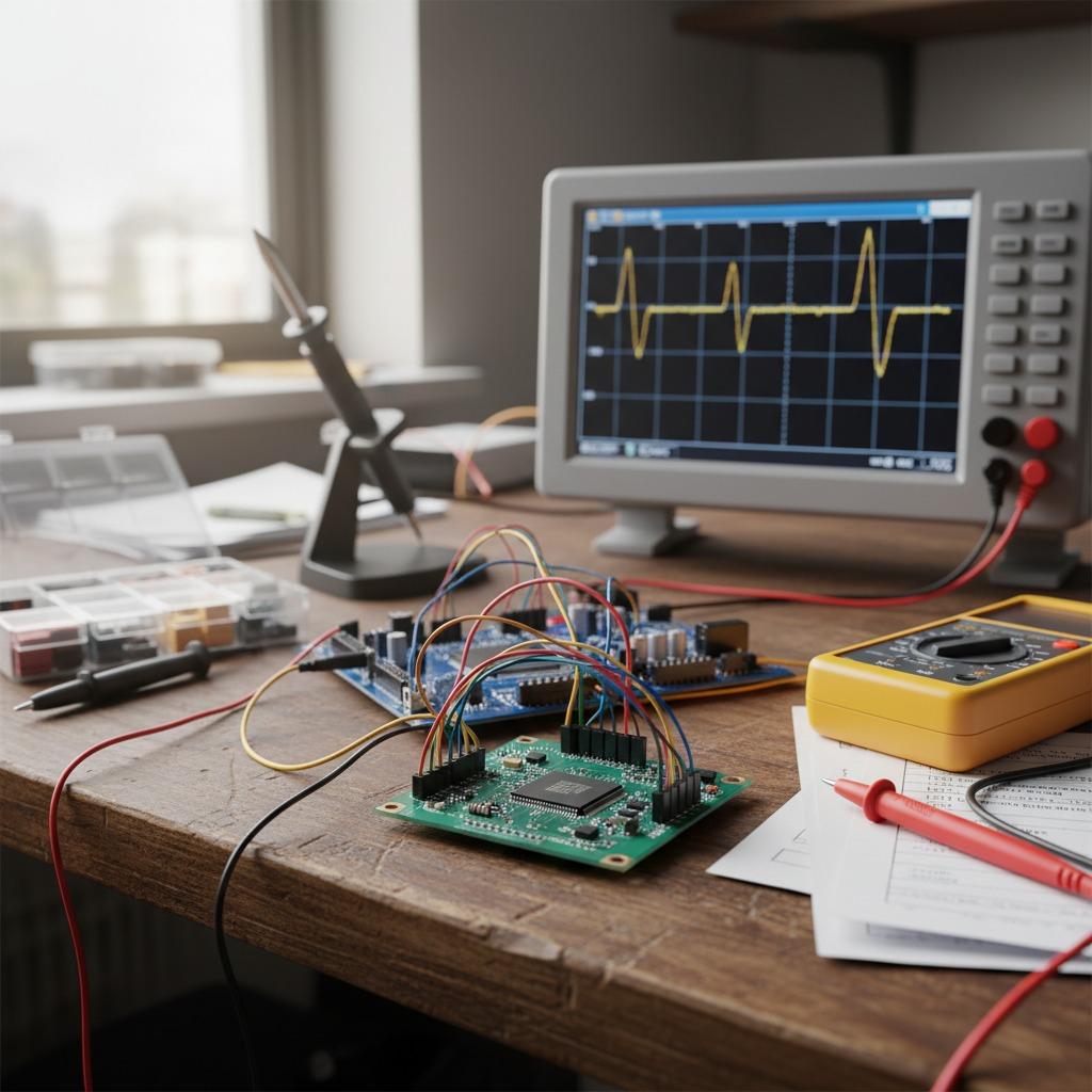
A WiFi Bluetooth PCBA is often treated like a small, ordinary board with two radios on it. In practice, it is a crowded piece of engineering where layout, assembly discipline, and test coverage matter just as much as the schematic. For smart products, the difference between a board that links up reliably and one that produces random disconnects can come down to details hidden under the solder mask: RF layout, antenna clearance, solder quality, and how cleanly the assembly line handles small, mixed-signal parts.
That is why buyers looking for a WiFi Bluetooth PCBA are usually not just buying assembly. They are making a decision about product stability, launch risk, and how much rework will be needed once the first batch comes off the line.
What this board has to do in real products
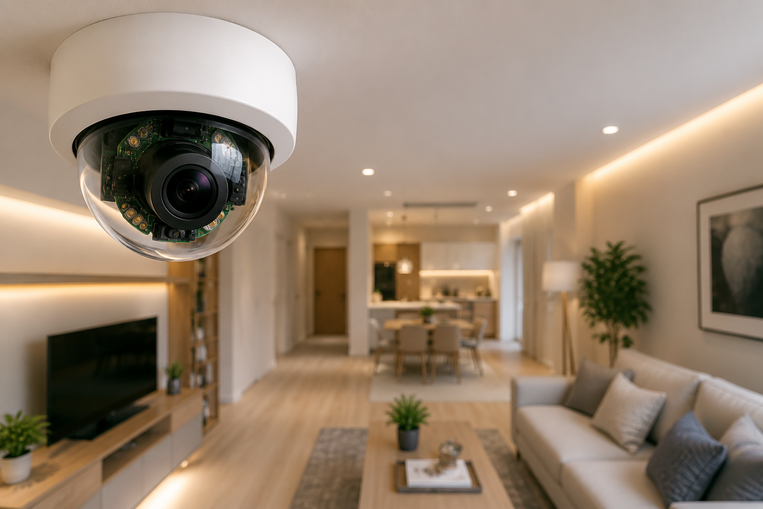
In a Smart Home PCB Assembly, the board may sit inside a thermostat, a light controller, a sensor hub, a gateway, or a voice-controlled appliance. A Home Automation Circuit Board has to do several jobs at once: keep wireless links stable, handle power cleanly, survive normal handling during assembly, and fit inside a tight enclosure that was probably designed by a mechanical engineer with very little spare room to give.
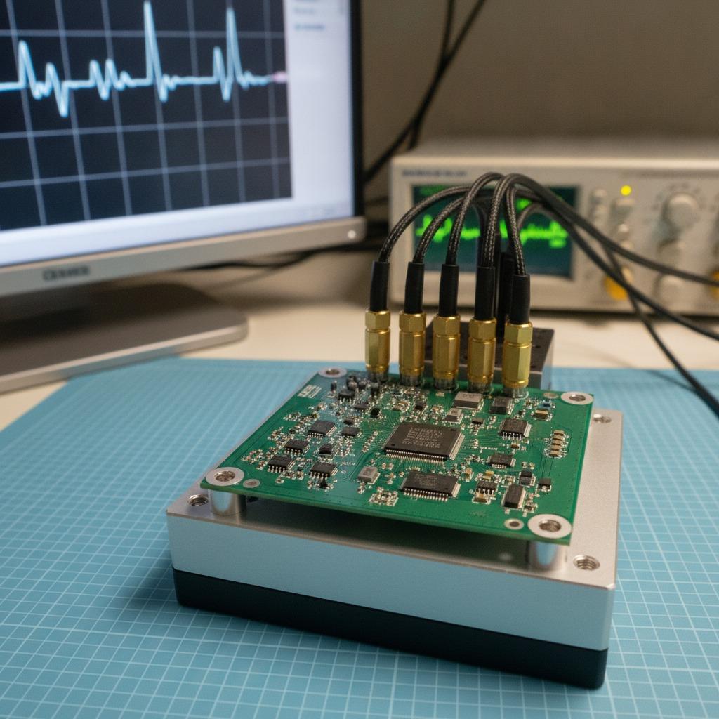
That is where the Smart Device Module concept matters. Many connected products are no longer built as loose prototypes with wires and daughter cards. They are expected to behave like finished modules, with repeatable soldering, dependable component sourcing, and test results that mean something from batch to batch.
Assembly details that make or break performance
For this kind of PCB assembly, the obvious work is only part of the story. SMT贴片 has to place small passive parts accurately, but it also has to respect the sensitive radio section. A careless paste stencil choice, uneven reflow profile, or poor component orientation can cause problems that show up later as intermittent RF behavior, weak connections, or heat-related failures.
hcdpcba lists SMT assembly, PCB prototyping, component sourcing, assembly, testing, and DFMA support as part of its service scope. That mix is useful because wireless boards often need more than a build-to-print approach. A design for a WiFi Bluetooth PCBA should be checked for manufacturability before the first panel goes into production. Traces around the antenna, grounding strategy, and component density near the RF section all deserve attention.
It is also worth noting a practical point: the better the board is designed for assembly, the less likely the production team will need to fight the design on the line. That sounds obvious, yet it is one of the most common sources of avoidable cost.
Key selection points for buyers
When sourcing a wireless board, buyers should compare suppliers on more than price. The first question is whether the factory can handle multi-layer boards, HDI boards, or high-frequency boards when the design calls for them. hcdpcba states that it supports these PCBA types, which matters for compact smart home products where routing space is tight.
The second question is sourcing control. Wireless products often depend on small ICs, passives, crystals, and connectors that look interchangeable on paper but are not interchangeable in the field. A supplier with component sourcing support can reduce the chance of receiving mismatched parts or inconsistent lots.
The third question is testing. For a Smart Device Module, assembly without adequate test is only half a job. Functional checks, connection verification, and process feedback help catch issues before they reach integration.
What to ask before placing an order
Ask whether the factory can support:
- PCB prototyping before mass build
- SMT assembly for small and mixed-density boards
- Component sourcing with a focus on genuine parts
- Assembly and testing under one roof
- DFMA review before production starts
If the answer is vague, the risk usually shows up later as schedule drift.
Common mistakes in wireless smart-home builds
The first mistake is overpacking the board. RF sections need breathing room, even when the enclosure does not. The second is assuming the same assembly route works for every revision. A board that was fine in a prototype run may need a changed stencil, different panelization, or stricter incoming inspection once volumes rise.
Another frequent problem is ignoring how enclosure materials, antenna position, and nearby metal affect performance. The PCB may be assembled correctly and still underperform if the mechanical integration is careless. Buyers should treat the board and enclosure as one system, not two separate purchases.
Practical advice for sourcing and production
For engineers and sourcing managers, the safest path is usually to start with a clear DFMA discussion, then confirm whether the factory can support both prototyping and repeat production. That is especially useful for IoT, smart home, and communications products, where revisions happen quickly and one board may have to serve several product variants.
hcdpcba positions itself around fast response, quality control, confidentiality, and OEM/ODM support. Those are broad claims, of course, and buyers should still verify the exact process fit for their own product. But a supplier that can handle PCB prototyping, SMT贴片, assembly, and testing under one roof is often easier to work with than a chain of disconnected vendors.
A simple next step
If you are planning a WiFi Bluetooth PCBA for a connected device, start by sending the design files, expected volumes, and any RF or enclosure constraints to the assembly partner. Ask for a manufacturability review before release. That one step can save more time than a rushed pilot run ever will.
For projects that need one-stop PCB assembly support, hcdpcba can be contacted at +86 18924624188 for discussion of prototype builds, SMT production, sourcing, assembly, and testing.