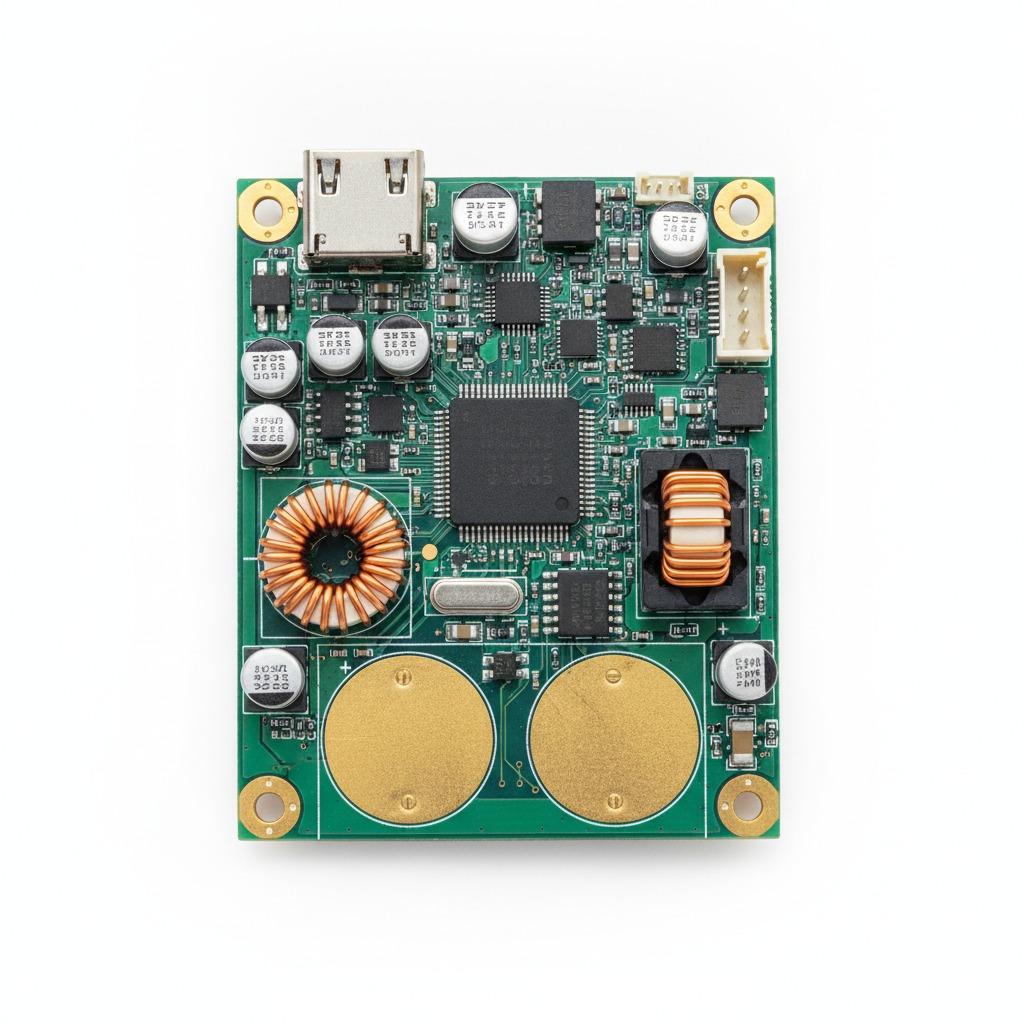
IoT PCBA Manufacturer for Scalable Connectivity and Long-Term Device Reliability
IoT products rarely fail because of ambition.
They fail because small technical decisions—made early and left unchecked—compound over time.
Unstable wireless performance, inconsistent power behavior, or component obsolescence do not always appear in prototypes. They surface months later, after devices are deployed across regions, environments, and usage patterns. At that point, correction becomes expensive.
This is why choosing an IoT PCBA manufacturer is less about short-term assembly capability and more about long-term production discipline that supports connectivity stability, lifecycle continuity, and controlled scaling.
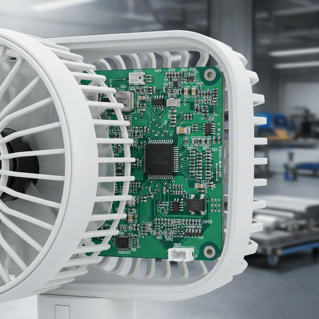
Why IoT PCBA Manufacturing Differs from General Electronics
IoT devices operate under constraints that many consumer electronics never face. They are often deployed remotely, updated infrequently, and expected to remain functional for years.
Key differences include:
-
Long product lifecycles with limited redesign windows
-
Dependence on wireless modules and antennas
-
Sensitivity to power fluctuation and noise
-
Fragmented volumes across multiple SKUs or regions
An experienced IoT PCBA manufacturer addresses these challenges through process and planning rather than post-deployment fixes.
Core Technical Challenges in IoT PCBA Production and How They Are Managed
IoT PCBA cost and reliability issues usually originate from a small set of technical weaknesses.
The most common challenges—and their control methods—include:
-
Wireless signal instability
Managed through controlled RF component placement, defined grounding strategies, and stable reflow profiles. Manufacturers that standardize RF-related assembly steps typically reduce field connectivity issues by 25–40% compared to ad-hoc layouts. -
Power fluctuation and sleep-mode inconsistency
Controlled by validating power sequencing and low-current states during production testing, not just during design validation. This reduces unexpected battery drain incidents by 15–30% in deployed devices. -
Component lifecycle risk
Addressed by qualifying long-availability components and alternates early, reducing mid-life redesign risk and avoiding forced substitutions that can disrupt performance.
These controls form the practical foundation of a capable IoT PCBA manufacturer.
Process Control for Connectivity-Centric Assembly
IoT devices are often tolerant of minor cosmetic defects but unforgiving of electrical inconsistency. Process control therefore focuses on functional stability rather than surface perfection.
Typical process controls include:
-
Locked assembly parameters for wireless modules
-
Defined solder profiles for low-power ICs
-
Controlled handling of antennas and RF shields
-
Standardized inspection focus on signal-critical areas
Manufacturers applying these controls consistently see 3–5% improvement in first-pass yield and fewer late-stage functional failures.
Sourcing Strategy and Lifecycle Planning for IoT Devices
IoT products scale gradually and remain in the market longer than most consumer electronics. Sourcing decisions must reflect this reality.
In structured IoT production:
-
Wireless modules are selected based on roadmap stability, not spot pricing
-
Approved alternates are validated before volume ramp
-
Forecast alignment reduces emergency procurement
An experienced IoT PCBA manufacturer typically helps customers achieve:
-
5–12% reduction in component-related cost volatility
-
Lower redesign frequency, improving overall program profitability
-
More predictable margins over multi-year deployments
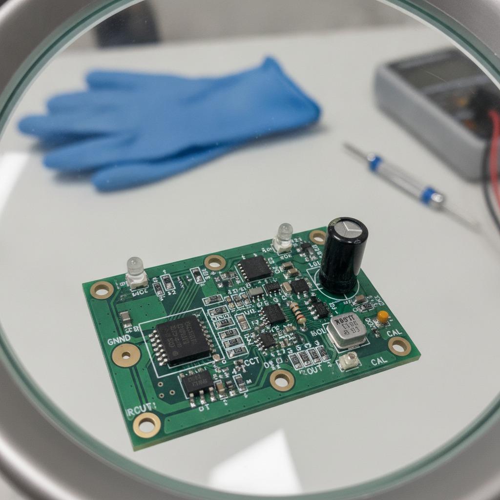
Testing and Validation Aligned with Real IoT Usage
Testing IoT devices requires more than basic power-on checks. Validation must reflect real operating conditions.
IoT-Focused Inspection and Testing Structure
| Test Stage | Applied Focus | Measured Benefit |
|---|---|---|
| In-line inspection | RF and power-critical areas | Early defect containment |
| Electrical testing | Power stability & signal paths | Functional consistency |
| Wireless sampling | Connectivity verification | Reduced field failures |
| Low-power mode check | Sleep & wake cycles | Battery life assurance |
| Trend analysis | Batch-to-batch data | Drift prevention |
By aligning testing depth with real deployment risks, manufacturers maintain reliability without inflating cycle time.
Where IoT PCBA Manufacturing Adds the Most Value
This manufacturing model is especially valuable in:
-
Smart home and building automation
-
Industrial monitoring and sensing
-
Asset tracking and logistics devices
-
Energy management and metering
In these applications, reliability over time is more valuable than short-term cost savings.
Frequently Asked Questions
Q1: Is IoT PCBA production suitable for low and medium volumes?
Yes. IoT products often scale gradually, making controlled production more important than sheer capacity.
Q2: How early should lifecycle sourcing be considered?
Ideally during pilot production. Early planning reduces forced changes later.
Q3: Does IoT manufacturing require specialized testing?
Yes. Wireless behavior and low-power operation must be validated beyond standard electrical tests.
Why Long-Term Thinking Matters in IoT Manufacturing
An IoT PCBA manufacturer does more than assemble boards. It supports connectivity stability, sourcing continuity, and predictable scaling over the full product lifecycle. When process control, testing alignment, and lifecycle planning work together, IoT devices remain reliable long after deployment.
If you are evaluating whether a manufacturer’s process structure can support IoT products at scale, reviewing real production capabilities and lifecycle planning approach is a practical first step. You can learn more about our PCBA manufacturing scope and technical strengths by visiting:
👉 https://www.hcdpcba.com
For projects that require a deeper discussion—such as wireless stability, lifecycle sourcing, or deployment-driven testing strategy—you are welcome to discuss your specific IoT PCBA requirements with our team here:
👉 https://www.hcdpcba.com/en/contact-us