Smart home products rarely fail because they are too complex.
They fail because they are expected to work quietly, continuously, and invisibly—often for years—inside environments that change every day.
Unstable WiFi connections, intermittent device resets, or inconsistent power behavior do not usually appear during early testing. They surface after deployment, when devices are installed in different homes, exposed to varying network quality, temperature, and electrical noise. At that stage, field fixes are expensive and reputation damage is difficult to reverse.
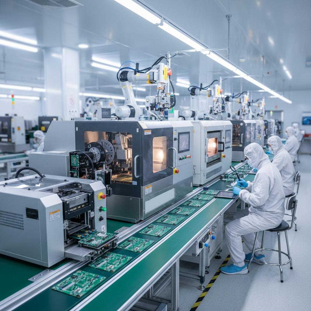
This is why smart home PCBA manufacturing is less about feature integration and more about disciplined production that ensures connectivity stability, electrical consistency, and long-term reliability at scale.
Why Smart Home PCBA Differs from General IoT Assembly
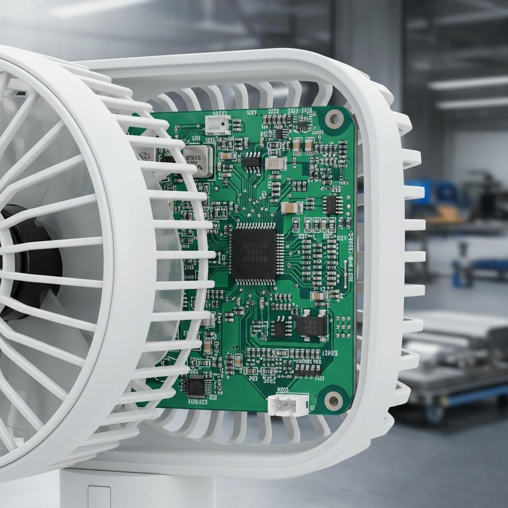
Smart home devices share the connectivity traits of IoT products, but their manufacturing requirements are more restrictive. Unlike industrial IoT equipment that operates in controlled environments, smart home devices must remain stable inside highly variable household conditions—different power grids, wireless interference levels, and user behaviors.
These differences introduce several manufacturing-specific challenges that must be addressed at the PCBA level.
1. Continuous operation under unstable power conditions
Smart home devices are often always-on or cycle frequently between active and standby states. Household voltage fluctuation and electrical noise can expose weaknesses in power management design and assembly quality.
To address this, smart home PCBA manufacturing requires tighter control of power-related solder joints, defined grounding paths, and validation of sleep–wake transitions during production testing. Manufacturers applying these controls typically reduce unexplained resets and lockups by 15–25% after deployment.
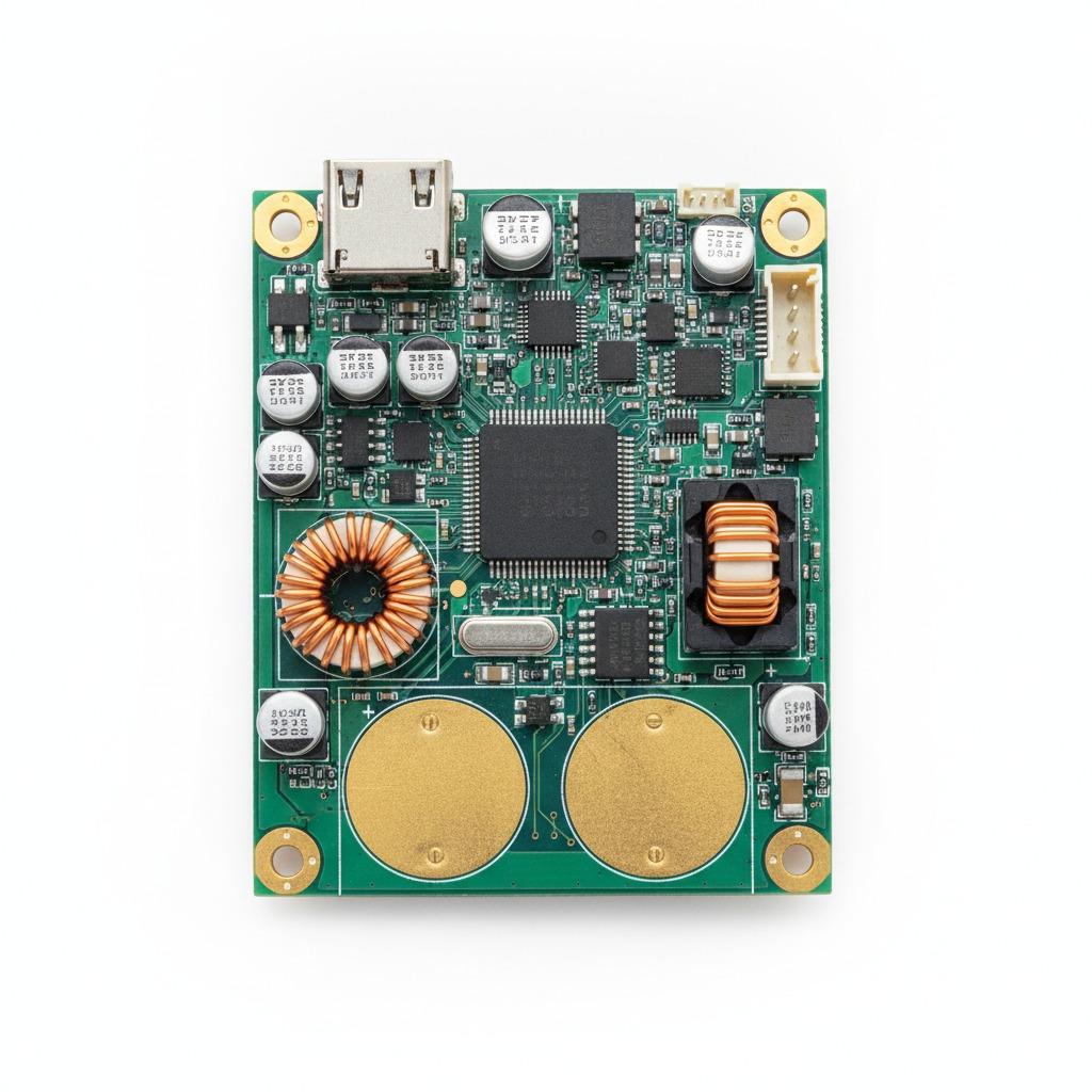
2. Wireless performance in interference-heavy environments
Unlike many IoT devices deployed in industrial settings, smart home products must coexist with dense WiFi traffic, Bluetooth devices, and consumer electronics. Minor variation in RF assembly can lead to inconsistent connectivity across homes.
Effective manufacturing control includes standardized placement of RF components, protected antenna handling, and inspection focus on signal-critical areas. When RF-related assembly steps are locked and audited, connectivity-related field complaints are reduced by 20–35%.
3. Long market presence with limited redesign opportunities
Smart home products often remain in the market for multiple years, while firmware updates replace hardware changes. This places greater importance on component lifecycle planning and sourcing stability.
An experienced smart home PCBA approach qualifies long-availability components and approved alternates early, reducing mid-life substitutions that can introduce unpredictable behavior or certification risk.
4. Fragmented SKUs driven by protocol and region
Smart home product lines frequently branch into multiple variants based on communication protocol or regional certification. Without disciplined process control, this fragmentation increases setup errors and cost leakage.
Manufacturers mitigate this by standardizing core assembly processes across variants and isolating differences only where necessary, improving changeover efficiency and reducing variant-related defects.
These factors explain why smart home PCBA manufacturing demands tighter process discipline than general IoT assembly. Stability is not achieved through additional features, but through manufacturing controls that anticipate real household conditions rather than ideal test environments.
Core Manufacturing Risks in Smart Home Devices and Practical Controls
Most reliability issues in smart home devices can be traced back to a limited number of manufacturing weaknesses.
The most common risks—and how they are addressed—include:
-
Wireless performance inconsistency
Controlled through defined RF component placement, grounding continuity, and protected antenna handling. Manufacturers applying standardized RF assembly rules typically reduce connectivity-related field issues by 20–35%. -
Power instability under real household conditions
Addressed by validating power behavior under voltage fluctuation and noise scenarios during production testing, reducing spontaneous resets by 15–25%. -
Component substitution across long product lifecycles
Mitigated by qualifying alternates early and selecting components with stable availability, avoiding mid-life changes that introduce unexpected behavior.
Together, these controls form the production backbone of a reliable smart home PCBA program.
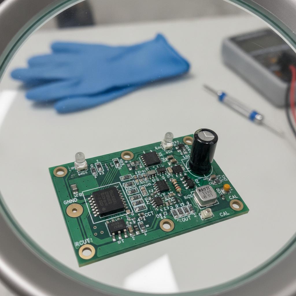
Process Control Focused on Connectivity and Power Stability
Unlike many consumer products, smart home devices are unforgiving of minor electrical variation. Process control therefore emphasizes stability rather than cosmetic perfection.
Typical controls include:
-
Locked assembly parameters for wireless modules
-
Defined solder profiles for power-management ICs
-
Controlled grounding paths across PCBAs
-
Inspection focus on signal- and power-critical zones
Manufacturers implementing these measures consistently report 3–6% improvement in first-pass yield and fewer late-stage functional failures.
Sourcing Discipline and Cost Stability in Smart Home Production
Smart home products often scale gradually and remain in the market for extended periods. Sourcing strategy must support this lifecycle.
In structured smart home PCBA manufacturing:
-
Wireless modules are selected based on roadmap stability, not short-term pricing
-
Approved alternates are validated before volume ramp
-
Forecast alignment reduces emergency purchasing
As production stabilizes, manufacturers commonly achieve:
-
5–10% reduction in component cost volatility
-
10–15% improvement in production predictability
-
More stable gross margins across multiple product variants
These gains are incremental but sustained over the product lifecycle.
Inspection and Testing Aligned with Real Home Usage
Testing must reflect real installation environments, not ideal lab conditions.
Smart Home–Focused Inspection and Testing Structure
| Test Stage | Applied Focus | Measured Impact |
|---|---|---|
| In-line inspection | RF & power-critical areas | Early defect detection |
| Electrical testing | Power stability & signal paths | Functional consistency |
| Wireless sampling | Network connectivity check | Reduced field issues |
| Sleep–wake validation | Power cycling behavior | Battery life stability |
| Trend analysis | Batch-level comparison | Drift prevention |
This approach balances reliability with production efficiency.
Where Smart Home PCBA Manufacturing Adds the Most Value
This manufacturing model is especially relevant for:
-
Smart lighting and switches
-
Home security and monitoring devices
-
Environmental sensors and controllers
-
Energy management and automation systems
In these applications, long-term stability matters more than short-term feature differentiation.
Why Manufacturing Discipline Defines Smart Home Reliability
A robust smart home PCBA strategy ensures that devices behave consistently across homes, networks, and regions. When process control, sourcing discipline, and usage-aligned testing work together, smart home products scale reliably without escalating cost or risk.
If you are evaluating whether a manufacturer’s production structure can support smart home devices at scale, reviewing real assembly processes and lifecycle planning is a logical first step. You can learn more about our PCBA manufacturing capabilities and technical scope by visiting:
👉 https://www.hcdpcba.com
For projects that require a more focused discussion—such as wireless stability, multi-SKU management, or long-term supply planning—you are welcome to discuss your requirements directly with our team here:
👉 https://www.hcdpcba.com/en/contact-us