Solar Hybrid Inverter PCB Board for Compact Power Control Systems
A solar hybrid inverter pcb board is the core electronics platform that helps a solar system manage power flow between panels, storage, loads, and control logic. For buyers, the challenge is usually not just making a board that fits the enclosure, but building a reliable assembly that can route signals cleanly, handle power components safely, and support stable operation in a compact energy system. In hybrid solar equipment, that balance matters because the PCB often sits inside a cabinet that must coordinate conversion, monitoring, and communication without wasting space or creating heat concentration.
Product Overview
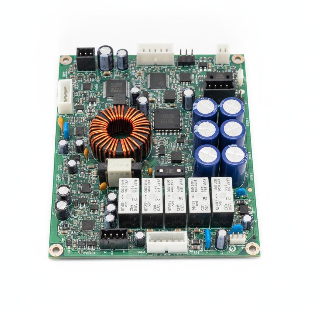
This type of board is typically a rigid printed circuit board assembly used in embedded power electronics or control modules. Based on the visible structure, the board features a green FR-4-style substrate, mixed surface-mount and through-hole components, a central processing or control IC, several support chips, capacitors, a toroidal inductor, a relay-like power component, and multiple connectors. The layout suggests a compact control platform intended for industrial electronics, energy equipment, or other systems where power handling and signal routing need to live on the same board.
In a solar cabinet or hybrid inverter environment, the pcb serves as the nervous system of the unit. It helps move signals between sensors, power stages, ports, and external wiring while keeping the circuit organized on a small footprint. The result is a cleaner build that is easier to assemble, test, and integrate into a finished housing.
Visible Structure and Key Capabilities
Compact mixed-technology assembly
The board shows a dense SMT layout with several through-hole parts. That combination is common in products that need both compact electronics and mechanically stronger components such as connectors, inductors, and relays. The plated mounting holes at the corners indicate the board is meant to be secured inside a cabinet or device frame.
Power-oriented component arrangement
The visible inductor, electrolytic capacitors, and relay-style block point to onboard power conditioning or switching functions. While the exact circuit cannot be confirmed from the image, these elements are typical of assemblies that manage regulation, filtering, or load control. For a solar inverter pcba, such placement helps reduce trace length and keeps the power section close to the supporting circuitry.
Connection and interface readiness
Multiple connectors and a USB-A style port suggest the board may support service access, communication, or integration with external modules. In practical terms, that makes the assembly more adaptable for control panels, embedded devices, or monitoring functions in energy hardware.
Materials and Finish Options
The visible base material appears to be FR-4 or a similar rigid laminate, which is widely used in industrial electronics for its mechanical stability and manufacturability. The board surface shows standard solder mask and exposed copper features under component pads and routed traces. For related builds such as a solar power pcb board, buyers often choose finishes and stackups according to electrical needs, assembly density, and environmental exposure. Since the image does not confirm layer count or coating type, those details should be defined during engineering review rather than assumed.
Manufacturing Process
This board category is generally produced through PCB fabrication followed by SMT assembly and selective through-hole soldering. The process usually begins with circuit design and DFM/DFMA review, then copper pattern fabrication, solder mask application, stencil printing, component placement, reflow soldering, and manual or automated insertion of larger parts. For a solar control pcba, final steps may also include inspection, electrical testing, and functional checks before installation into an enclosure.
hcdpcba supports SMT贴片, PCB打样, component sourcing, assembly, testing, OEM, and ODM services, which is useful when a buyer needs both prototyping and production support under one workflow.
Application Scenarios
Although the exact function is not identifiable from the image alone, the visible design fits several common use cases:
Industrial controllers and automation modules
Embedded computing or communication boards
IoT hardware and sensor interface systems
Solar hybrid inverter cabinets and monitoring electronics
Battery or power management modules
Prototype systems where power regulation and signal routing share one compact assembly
Quality Control and Buyer Decision Factors
When selecting a solar inverter pcb board or similar control assembly, buyers usually evaluate electrical layout quality, soldering consistency, connector reliability, and the ability to fit the enclosure and thermal design. Visual density alone is not enough; the real value comes from stable assembly, trace discipline, component sourcing, and verification testing. For outdoor or energy-related use, cabinet integration and wiring discipline are equally important because cable paths, vibration, and heat can influence long-term performance.
Key questions to confirm during procurement include board dimensions, layer count, copper weight, component substitutions, test coverage, firmware needs, and whether the build must support small-batch prototyping or volume production. If the board will be used in a solar hybrid inverter pcb board project, it is also smart to review thermal paths, mounting method, service access, and any required communication interfaces before release.
Customization Guidance
Custom PCBAs in this category are usually adapted by changing connector placement, power stage parts, interface ports, mounting holes, or the control chipset. Buyers may also request integrated testing, component procurement, or a revised layout for easier assembly. For projects that sit inside a solar cabinet, routing and spacing should be reviewed early so the finished board can be mounted cleanly with short wiring runs and minimal rework.
Why Work with hcdpcba
hcdpcba provides SMT贴片, PCB打样, 元器件代采, 组装, 测试, DFMA analysis, OEM, and ODM support. That makes the company a practical partner for buyers who need a solar hybrid inverter pcb board concept moved from layout to assembly with fewer handoffs. The combination of technical support and production flexibility is especially useful for industrial electronics, power systems, and custom embedded hardware.
Request a Quote
If you are planning a control board, inverter module, or custom solar power pcb board project, send your schematic, BOM, Gerber files, or sample requirements for review. A clear engineering brief helps confirm manufacturability, component sourcing, and the right assembly path before production begins.