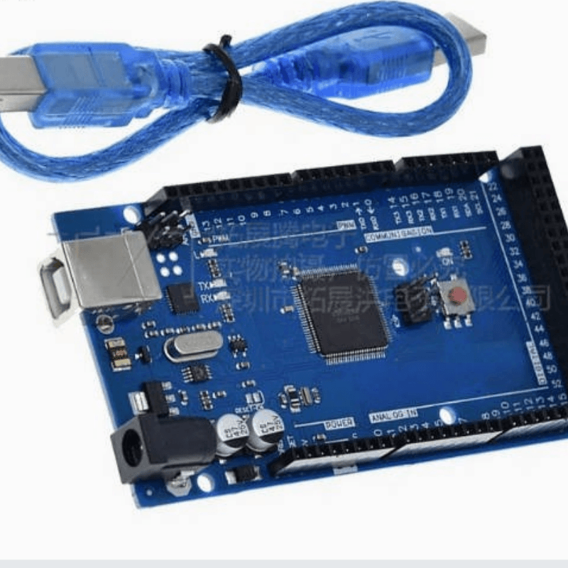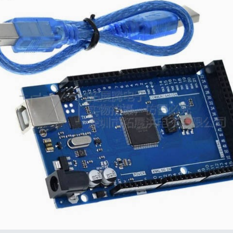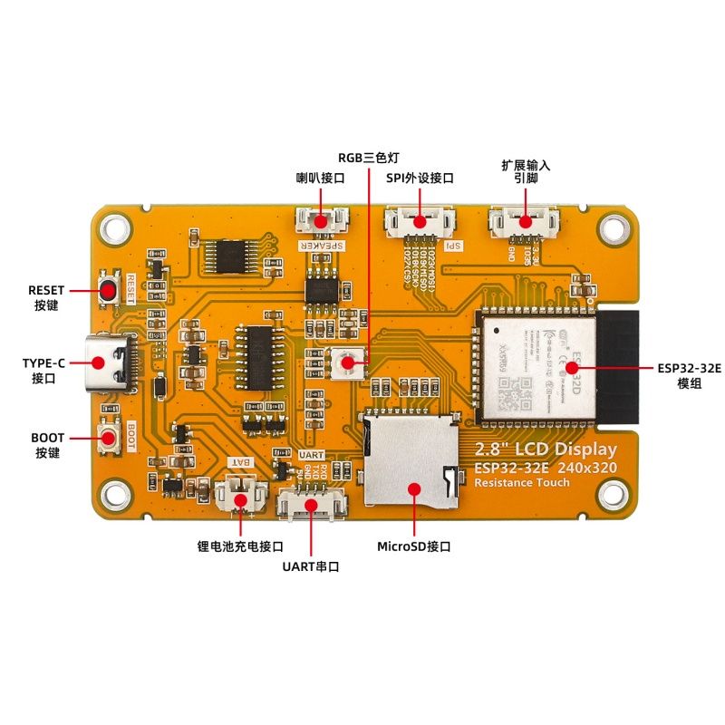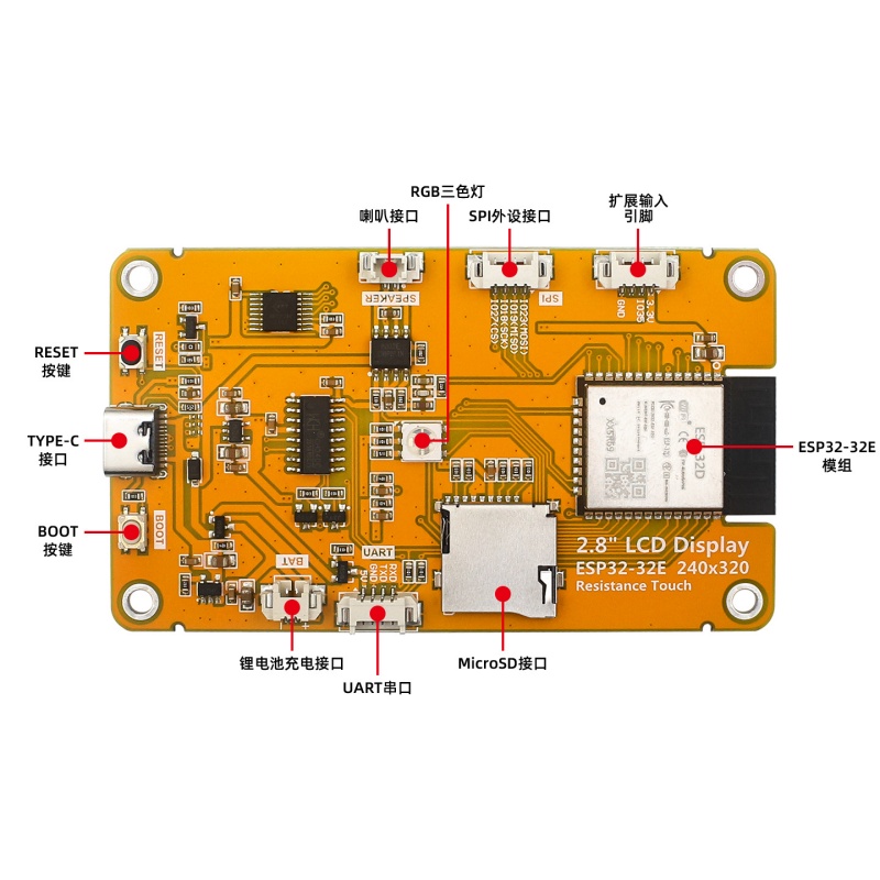
In the fast-paced world of modern electronics, the Network Interface PCB stands as a cornerstone of reliable connectivity and high-performance data transmission. At hcdpcba, we pride ourselves on delivering cutting-edge solutions that bridge the gap between innovation and practicality. This advanced Network Interface PCB is meticulously engineered to handle the demands of today's interconnected devices, featuring a robust design that ensures seamless integration into various applications. With its sleek blue substrate and intricate network of conductive pathways, it optimizes signal integrity while minimizing electromagnetic interference, making it an essential component for networking hardware.
Delving deeper into its capabilities, our Network Interface PCB incorporates high-density integration, allowing for compact yet powerful layouts that support complex functionalities without compromising on space. The centerpiece is a state-of-the-art microchip that drives superior processing speeds, enabling faster data routing and enhanced multitasking in demanding environments. Precision components, including gold-plated connectors and reliable resistors, work in harmony to ensure efficient energy transfer and corrosion resistance, prolonging the lifespan of your devices. Whether you're developing smart home systems or industrial automation tools, this PCB elevates performance by reducing power consumption and boosting overall efficiency. hcdpcba's expertise in SMT贴片 and PCBA板 production ensures that every board meets stringent quality standards, drawing from our comprehensive services like PCB打样 and 元器件代采 to deliver tailored solutions.
What sets our Network Interface PCB apart is its seamless compatibility with Optical Communication PCB Assembly, a related technology that amplifies its potential in fiber-optic networks. This assembly process, honed through hcdpcba's years of experience in multi-layer and HDI boards, facilitates high-speed optical data transfer with minimal latency. Imagine deploying this in telecommunications or IoT applications, where the PCB's premium conductors and inductors ensure pristine signal quality over long distances. Our Optical Communication PCB Assembly supports diverse industries, from medical devices to automotive electronics, providing the durability needed for harsh conditions. With services like DFMA analysis and OEM/ODM customization, we optimize designs to lower costs and accelerate time-to-market, all while maintaining strict quality controls and confidentiality.
At hcdpcba, innovation meets reliability in every Network Interface PCB we produce. Our technical team, backed by advanced production lines, handles everything from small-batch prototyping to large-scale manufacturing, ensuring zero defects and rapid response times. Clients in communications, artificial intelligence, and power sectors trust us for our cost-effective approaches and one-stop solutions. Upgrading to this Network Interface PCB means embracing a future where connectivity is not just functional but transformative. Contact us at +86 18924624188 to explore how our Optical Communication PCB Assembly can integrate with your projects, driving efficiency and excellence across your operations.
The versatility of the Network Interface PCB extends to emerging fields like smart grids and security systems, where its thermal management features prevent overheating during intensive use. Paired with our testing services, every unit undergoes rigorous validation to guarantee peak performance. hcdpcba's commitment to customer satisfaction shines through in our ability to procure authentic components and assemble with precision, reducing risks and enhancing product reliability. As we continue to push boundaries in microelectronics, this PCB represents more than hardware—it's a gateway to smarter, more connected worlds, ready to power your next breakthrough.
Loading...