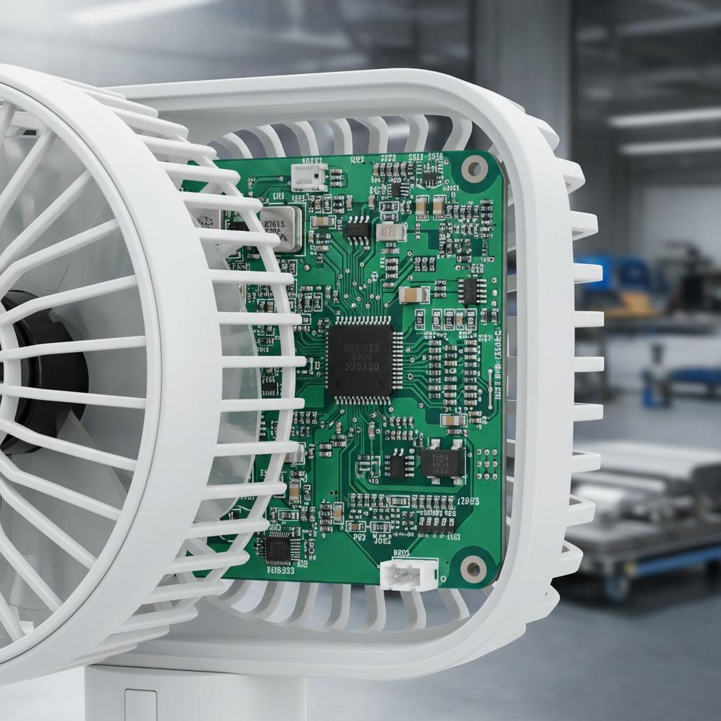
Power supply boards become significantly more difficult to manufacture once power components are packed closely together.
As layouts grow denser, thermal coupling increases, solder behavior becomes less forgiving, and small assembly variations begin to affect electrical performance over time rather than immediately.
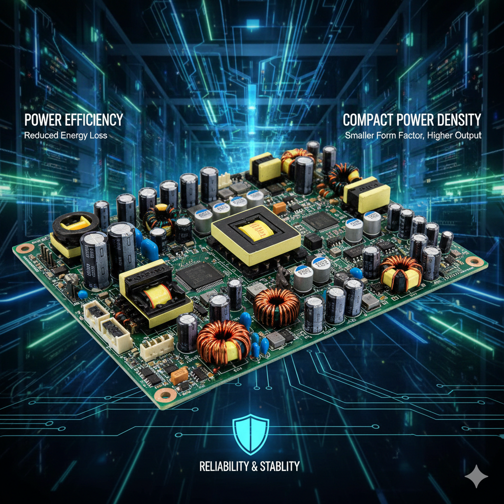
In this context, Power Supply PCBA Manufacturing for Boards with Dense Power Components is not about fitting parts onto a board. It is about controlling how current, heat, and mechanical stress interact inside a limited physical space—consistently, across batches, and under real operating conditions.
Why Dense Power Component Layouts Change Manufacturing Risk
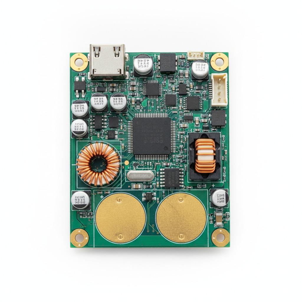
Dense power layouts concentrate MOSFETs, inductors, transformers, rectifiers, and bulk capacitors into compact areas. This concentration amplifies manufacturing sensitivity.
Typical risks introduced by dense power designs include:
-
Uneven solder distribution on thermally massive components
-
Localized heat accumulation during reflow and operation
-
Increased stress on solder joints during thermal cycling
-
Greater sensitivity to placement offset and coplanarity variation
Without targeted manufacturing controls, these risks often translate into drift in output stability, rising field failure rates, or shortened component lifespan.
Assembly Control Strategies for Dense Power Areas
In Power Supply PCBA Manufacturing for Boards with Dense Power Components, assembly control must be more granular than in standard power boards.
Key control measures include:
-
Stencil and solder volume optimization for mixed thermal mass components to avoid insufficient wetting or excessive solder voiding
-
Placement force and speed control for heavy or tall power components to maintain coplanarity
-
Component-specific reflow profiling that accounts for copper thickness and local heat absorption
Manufacturers applying these controls typically observe:
-
15–25% reduction in solder-related defects in dense power zones
-
More consistent electrical parameters across production batches
These improvements directly reduce downstream rework and performance variance.
Thermal Balance as a Manufacturing Responsibility
Thermal behavior in dense power boards is not defined solely by design. Assembly execution plays a decisive role.
Minor variation in solder thickness or component seating can alter heat dissipation paths, leading to uneven temperature distribution during operation. Over time, this accelerates aging of stressed components.
Effective Power Supply PCBA Manufacturing for Boards with Dense Power Components includes:
-
Locking reflow profiles validated for high thermal mass areas
-
Inspecting solder joints on power devices beyond visual criteria
-
Maintaining placement accuracy to preserve intended thermal conduction
Programs with these measures in place often achieve:
-
10–20% reduction in operating temperature variance
-
Improved long-term stability under continuous load
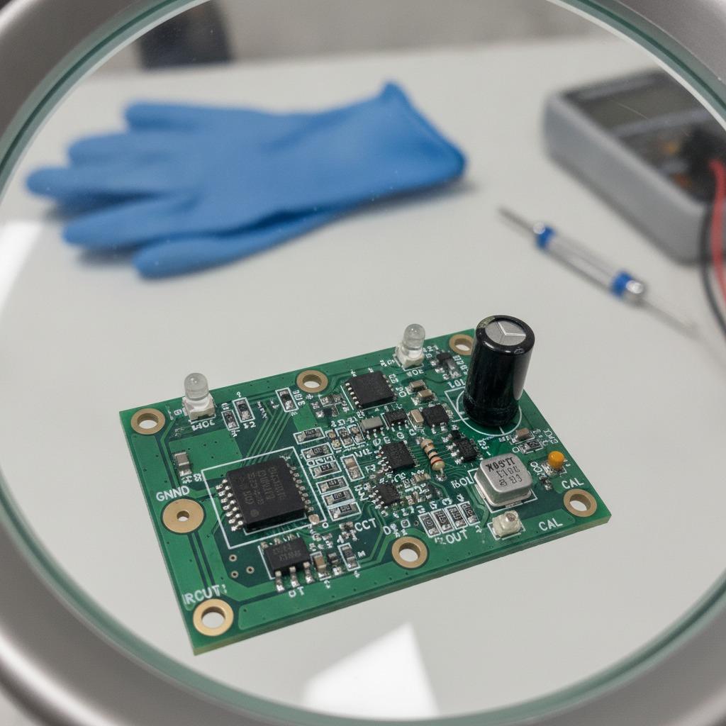
Inspection and Validation Focused on High-Density Power Areas
Inspection must prioritize functional risk, not cosmetic uniformity.
Dense Power–Focused Inspection and Validation Structure
| Validation Stage | Applied Scope | Reference Impact |
|---|---|---|
| In-line inspection | Dense power component zones | 20–30% fewer latent solder defects |
| AOI tuning | Power device leads & pads | Improved defect detection accuracy |
| Electrical testing | Load regulation & ripple | Early instability identification |
| Thermal observation | Hot-spot distribution | Reduced localized overheating |
| Trend analysis | Batch-to-batch comparison | Prevents gradual performance drift |
These steps help ensure that dense power layouts behave consistently after deployment, not just at shipment.
Scaling Production Without Amplifying Density-Related Issues
As volumes increase, the risks associated with dense power layouts compound. Small assembly deviations that were acceptable at low volume become systemic at scale.
In disciplined Power Supply PCBA Manufacturing for Boards with Dense Power Components:
-
Assembly parameters validated during pilot runs are locked before scale-up
-
Approved alternates for power components are qualified under load
-
Yield and thermal data are monitored continuously rather than reactively
Manufacturers following this approach typically experience:
-
10–20% fewer density-related failures after volume ramp
-
More predictable yield across extended production runs
Where Dense Power PCBA Manufacturing Matters Most
This manufacturing capability is especially critical for:
-
Compact AC–DC and DC–DC power supplies
-
High-efficiency power modules
-
Embedded power boards with space constraints
-
Industrial and energy systems with high power density
In these applications, consistency and thermal predictability matter more than minimizing board size alone.
Frequently Asked Questions
Q1: Are dense power boards always higher risk to manufacture?
They are more sensitive, but risk can be controlled through disciplined assembly and validation.
Q2: Can standard reflow profiles handle dense power layouts?
Often not. Dense power areas typically require profile optimization to ensure uniform solder behavior.
Q3: Does dense component placement affect long-term reliability?
Yes. Without proper thermal balance, component stress increases over time.
Why Dense Power Layouts Demand Manufacturing Discipline
Power Supply PCBA Manufacturing for Boards with Dense Power Components requires more than standard assembly capability. It demands precise control of solder behavior, thermal balance, and batch-to-batch consistency. When these factors are managed deliberately, compact power designs can scale reliably without hidden performance penalties.
If you are evaluating whether a manufacturer can support dense power supply boards at scale, reviewing real assembly controls and validation methods is an essential first step. You can learn more about our PCBA manufacturing capabilities and technical scope by visiting:
👉 https://www.hcdpcba.com
For projects that involve compact layouts, high power density, or long-duty-cycle operation, discussing your specific power board requirements directly often reveals where manufacturing discipline makes the biggest difference. You are welcome to contact our team here:
👉 https://www.hcdpcba.com/en/contact-us