Exploring the World of Wireless Communication PCBs
In the rapidly evolving landscape of modern electronics, the wireless communication PCB stands as a cornerstone of innovation, enabling seamless connectivity in devices that power our daily lives. At hcdpcba, we specialize in crafting these essential components with precision and expertise, drawing on our extensive experience in PCB design and manufacturing. Our wireless communication PCBs are engineered to handle high-frequency signals with remarkable efficiency, ensuring reliable data transmission in everything from smartphones to IoT networks. This technology not only bridges the gap between devices but also paves the way for smarter, more interconnected systems.
The Intricate Design of Wireless Communication PCBs
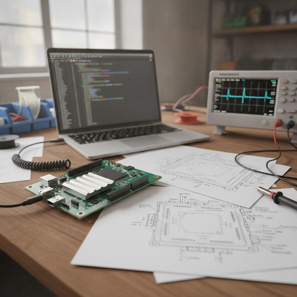
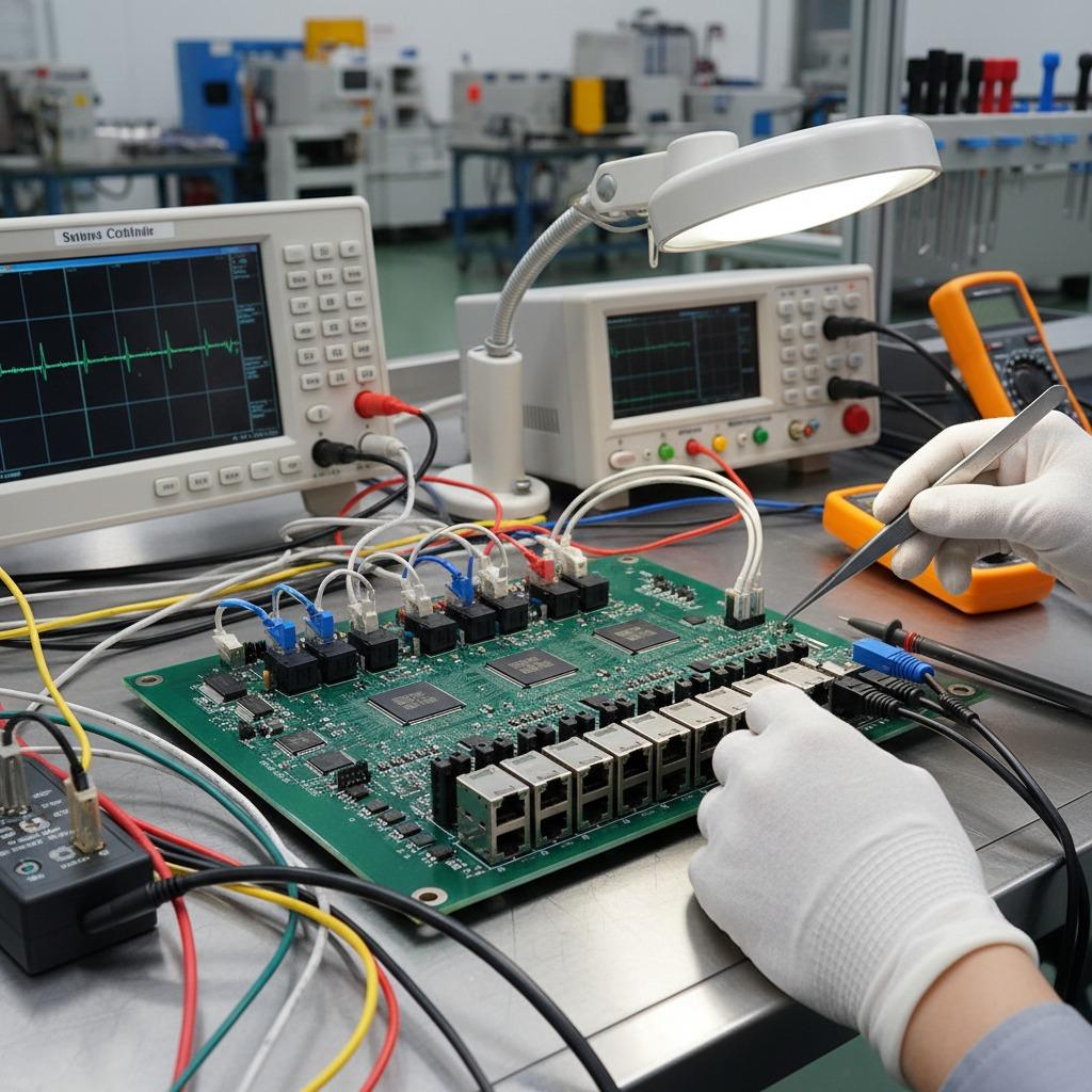
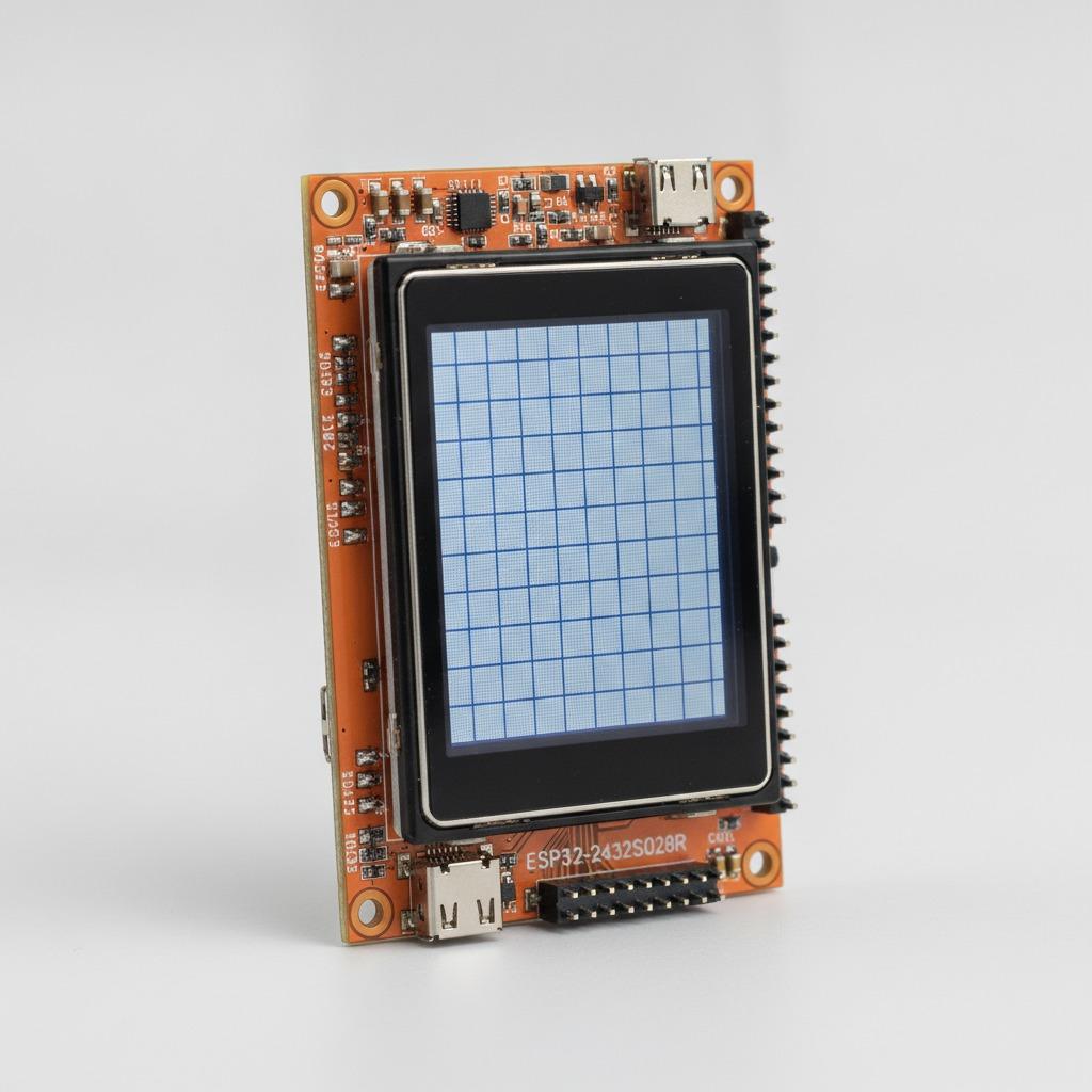
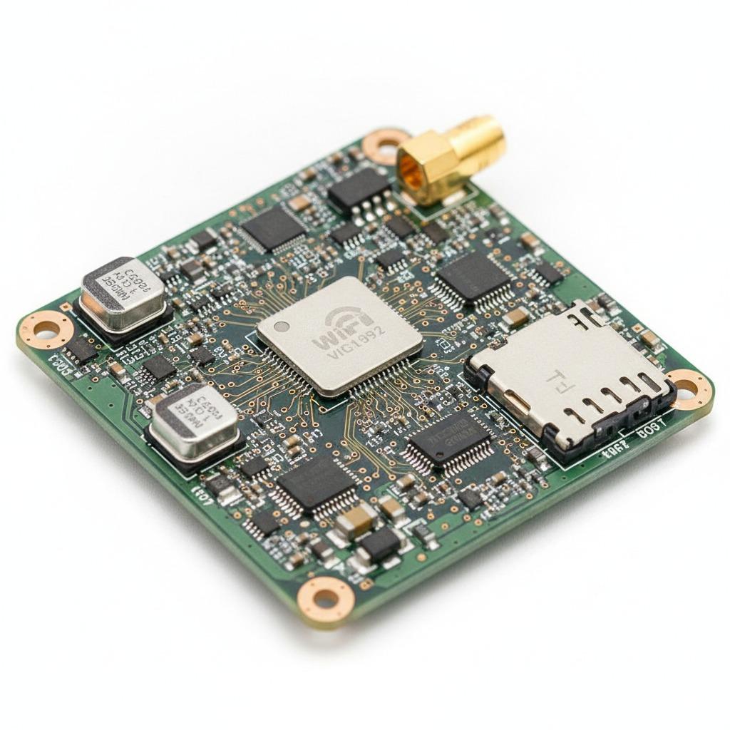
Imagine a compact, vibrant green board alive with intricate pathways of copper traces, each one meticulously routed to facilitate the flow of wireless signals without interference. Our wireless communication PCB at hcdpcba features advanced multilayer constructions, incorporating high-frequency materials that minimize signal loss and enhance bandwidth. Surface-mounted components, including antennas and RF modules, are precisely placed to optimize performance, creating a symphony of electrical harmony. This design prowess allows for the integration of complex circuits in limited spaces, making it ideal for portable gadgets where every millimeter counts. With our commitment to quality, these boards undergo rigorous testing to withstand environmental stresses, ensuring longevity and dependability in real-world applications.
Satellite Communication PCBs: Reaching for the Stars
Venturing into more specialized realms, our satellite communication PCB takes wireless technology to extraordinary heights, designed to endure the harsh conditions of space while maintaining crystal-clear links with Earth-based stations. Picture a robust board fortified with radiation-resistant laminates and shielded traces that combat electromagnetic interference from cosmic sources. At hcdpcba, we leverage our expertise in high-density interconnects (HDI) to build these satellite communication PCBs, supporting applications in global positioning systems and deep-space probes. The vivid array of connectors and mounting points ensures seamless assembly into satellite payloads, where reliability is non-negotiable. Our one-stop services, from PCB prototyping to full assembly and testing, empower aerospace engineers to innovate without compromise, delivering products that connect worlds.
Power Amplifier PCBs: Amplifying Connectivity
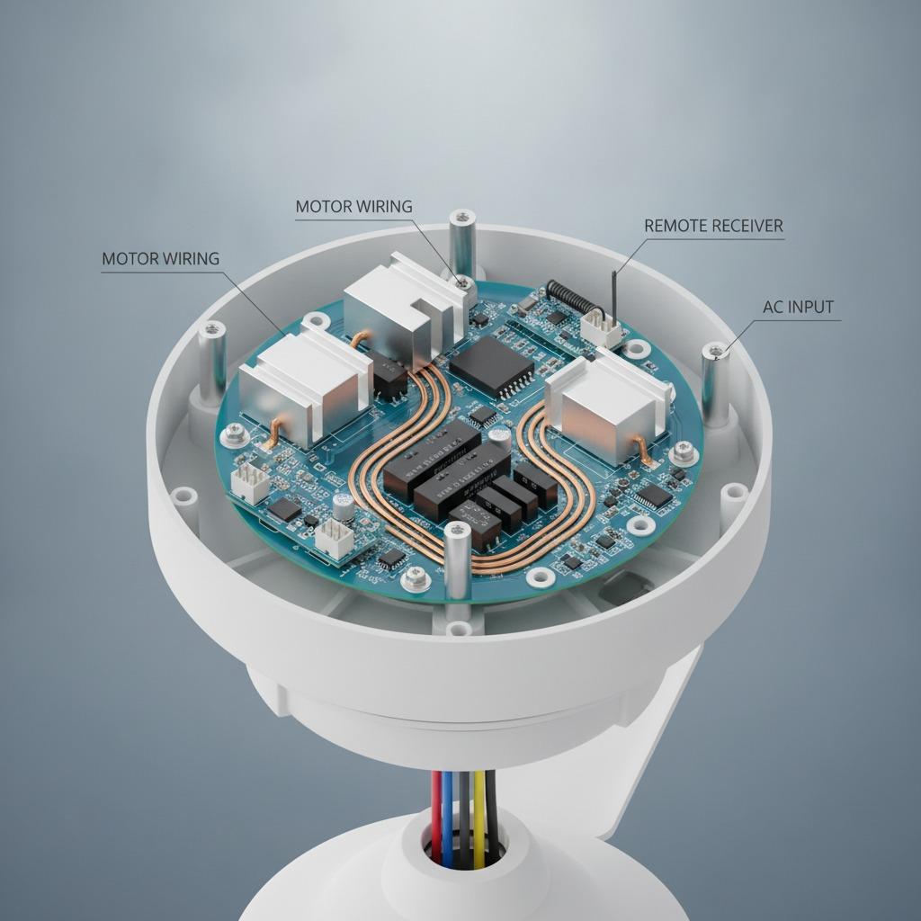
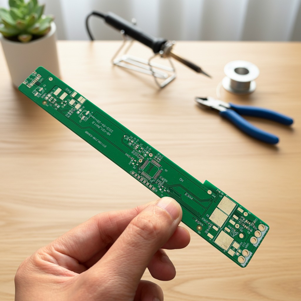
At the heart of powerful wireless signals lies the power amplifier PCB, a dynamic component that boosts transmission strength for clearer, farther-reaching communications. Envision a board pulsating with energy-efficient amplifiers and heat-dissipating layers, crafted to handle high power outputs without overheating. hcdpcba's power amplifier PCBs are tailored for demanding environments, such as base stations and wireless routers, where signal integrity can make or break connectivity. We incorporate advanced thermal management techniques and impedance-controlled traces to maximize efficiency, reducing energy consumption while enhancing output. Through our DFMA services, we optimize designs for manufacturability, cutting costs and accelerating time-to-market for our clients in telecommunications and beyond.
Why Choose hcdpcba for Your PCB Needs
What sets hcdpcba apart is our holistic approach to electronic manufacturing, blending cutting-edge technology with personalized service. From SMT placement that ensures pinpoint accuracy to comprehensive testing that validates every function, we cover the entire production spectrum. Our OEM and ODM capabilities allow for custom solutions in wireless communication PCB, satellite communication PCB, and power amplifier PCB projects, serving industries like IoT, automotive electronics, and medical devices. With a responsive team ready to quote and produce swiftly—contact us at +86 18924624188—we guarantee confidentiality, cost savings, and zero-defect quality. Whether you're prototyping a groundbreaking device or scaling production, our PCBs bring your visions to life, fostering innovation that resonates across applications.
In embracing these advanced PCBs, hcdpcba continues to drive the future of wireless technologies, where every connection tells a story of precision and possibility.