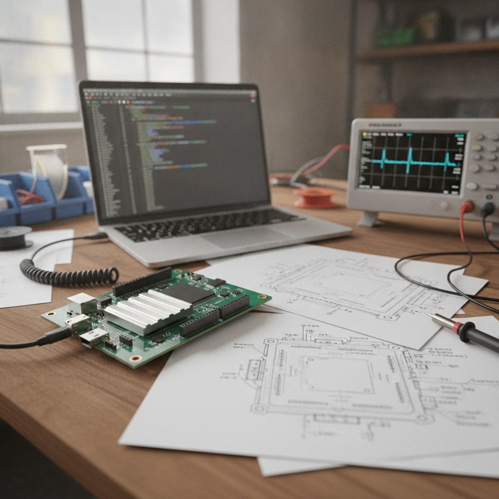
Many electronics projects become expensive not because the initial quote is high, but because hidden cost appears later. Yield loss, repeated rework, emergency component sourcing, excessive inspection, and unstable production transfer can quietly increase total manufacturing expense.
A structured PCBA cost optimization approach solves this by reducing waste at the source. Instead of cutting inspection or choosing the cheapest materials, HCDPCBA focuses on BOM review, SMT process control, sourcing discipline, and testing alignment to help customers lower cost while keeping production stable. You can also review our company background through the About Us page.
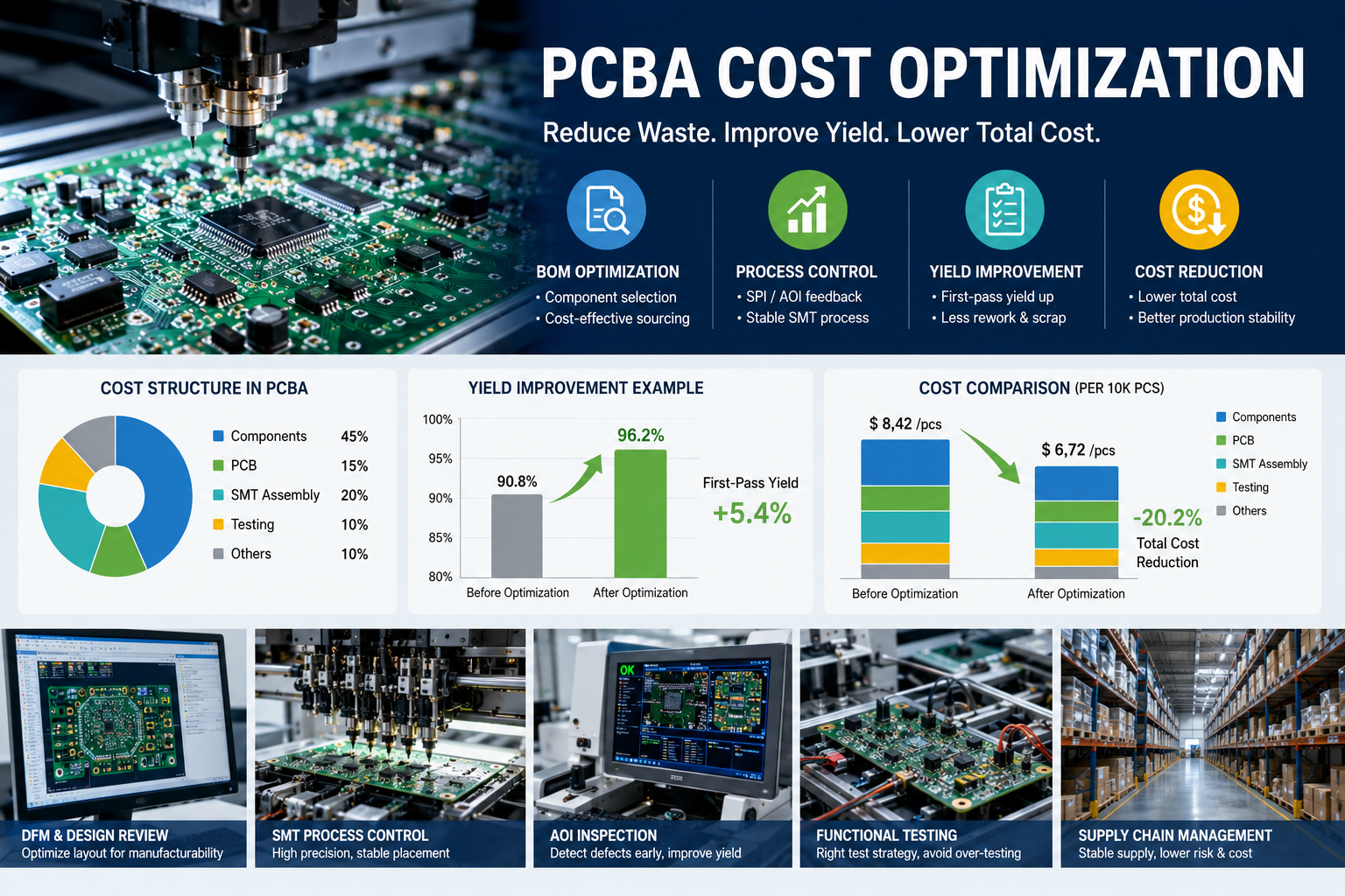
Why PCBA Cost Optimization Starts Before Production
Cost control begins before SMT assembly. If the BOM includes hard-to-source parts, if the PCB layout is difficult to assemble, or if test requirements are not defined early, the production line will absorb those problems later.
For example, a fine-pitch component layout with poor spacing may increase solder bridge defects. A power board without thermal balance may require extra testing and rework. These problems are not solved by asking for a lower unit price; they require process-level correction.
A practical PCBA cost optimization plan usually starts with three checks: BOM availability, DFM review, and assembly risk analysis. For PCBA-related product capabilities, you can refer to our PCBA Products page.
Key Cost Drivers and Practical Solutions
The biggest cost drivers in PCBA manufacturing are usually predictable. Yield loss often comes from solder paste inconsistency, placement deviation, or unstable reflow profiles. Sourcing cost rises when substitute components are chosen too late. Testing cost increases when every board is over-tested without risk classification.
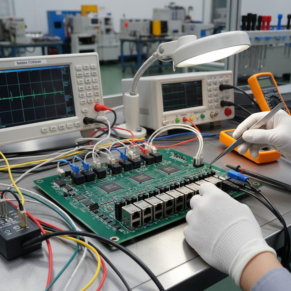
The solution is not one single action. Effective PCBA cost optimization combines stencil design improvement, SPI/AOI feedback, approved alternates, and targeted functional testing. In stable production environments, closed-loop SPI and AOI can improve first-pass yield by 3–8%, while recurring rework can often be reduced by 20–35% after process tuning.
Technical Parameters Buyers Should Review
| Parameter | Typical Reference Range | Cost Impact |
|---|---|---|
| PCB Layers | 2–12 layers | Higher layer count increases material and process cost |
| Copper Weight | 1–3 oz | Higher copper improves current capacity but raises fabrication cost |
| SMT Placement Accuracy | ±0.025–0.05 mm | Better accuracy reduces fine-pitch defects |
| Reflow Peak Temperature | 235–250°C | Stable profiles reduce solder joint failure |
| First-Pass Yield Target | 95–98%+ | Higher yield reduces rework and delivery risk |
These parameters help buyers understand whether a supplier is only quoting cheaply or actually controlling cost through manufacturing discipline.
Standard Cost Cutting vs Structured Cost Optimization
| Approach | Standard Cost Cutting | Structured Optimization |
|---|---|---|
| Component sourcing | Cheapest available parts | Approved alternates with lifecycle review |
| Inspection | Reduced testing to save time | Risk-based SPI, AOI, and functional testing |
| Process control | Adjusted during production | Locked after pilot validation |
| Result | Lower upfront price, higher risk | Lower total cost, more stable output |
This comparison is important for OEM buyers. A low quote may look attractive, but unstable yield and late-stage rework can erase the savings quickly.
Where This Approach Works Best
This approach is especially useful for industrial controllers, IoT devices, power supply boards, camera modules, AI hardware, and long-term OEM production. These products usually require stable repeat orders, controlled sourcing, and predictable quality across batches.
For common buyer questions about production, quality, and delivery, the FAQ page can help clarify basic cooperation details before starting a project.
Frequently Asked Questions
Q1: Can cost be reduced without redesigning the PCB?
Yes. Process optimization, sourcing control, and inspection strategy can reduce total cost even when the PCB design remains unchanged.
Q2: What is the biggest hidden cost in PCBA production?
Recurring defects are often the largest hidden cost because they create rework, delays, material waste, and engineering troubleshooting time.
Q3: Is cheaper component sourcing always better?
No. Unverified substitutes may create electrical variation, certification risk, or long-term reliability problems.
Why Cost Control Must Be Built Into the Manufacturing System
PCBA cost optimization is not simply about lowering unit price. It is about reducing waste, stabilizing yield, and preventing avoidable production problems before they become expensive. When BOM planning, assembly control, inspection strategy, and sourcing discipline work together, manufacturers can reduce total cost while maintaining stable product quality.
For teams evaluating long-term PCBA production, reviewing manufacturing capability and product scope is a practical first step through HCDPCBA. For specific cost-reduction analysis, BOM review, or production planning, you can contact the team through Contact Us.