The Heart of Modern Electronics
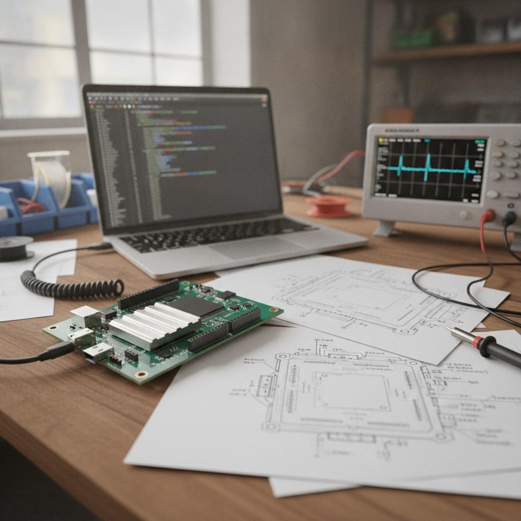
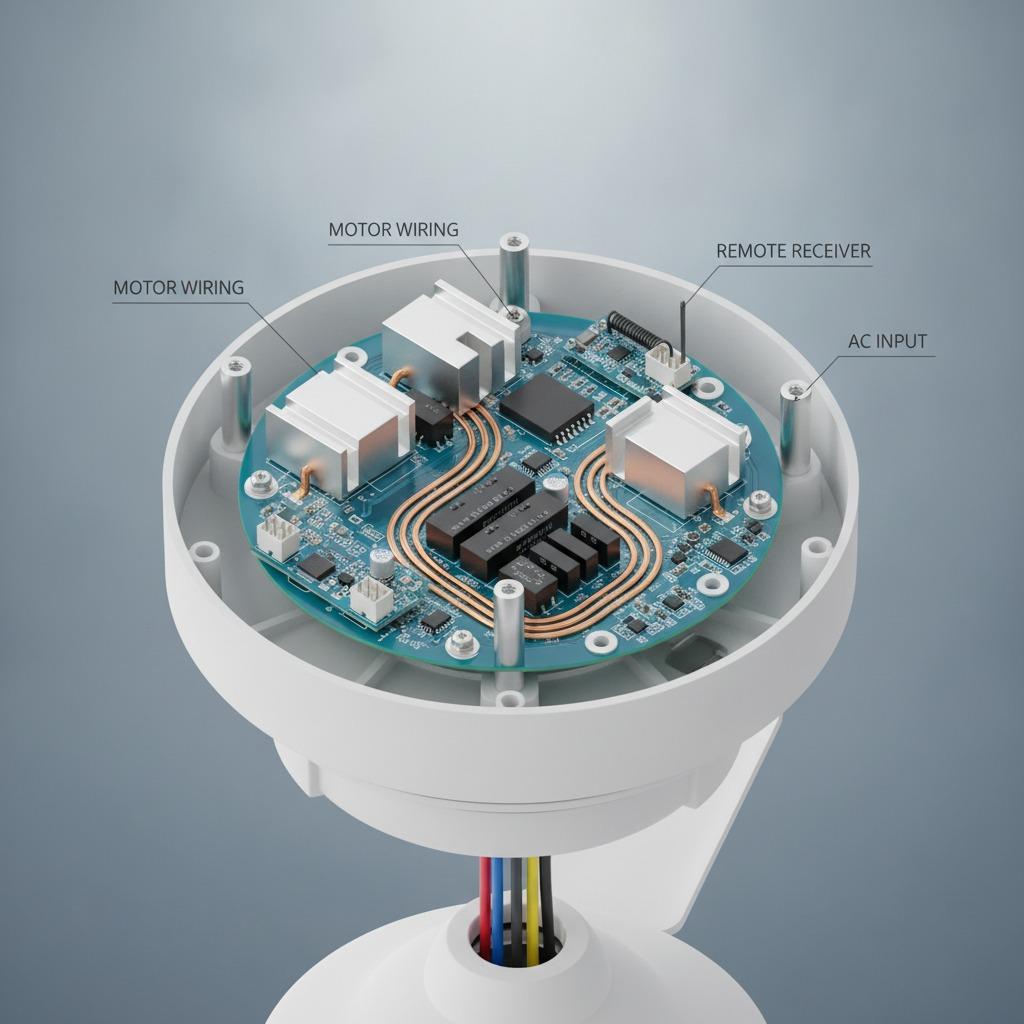
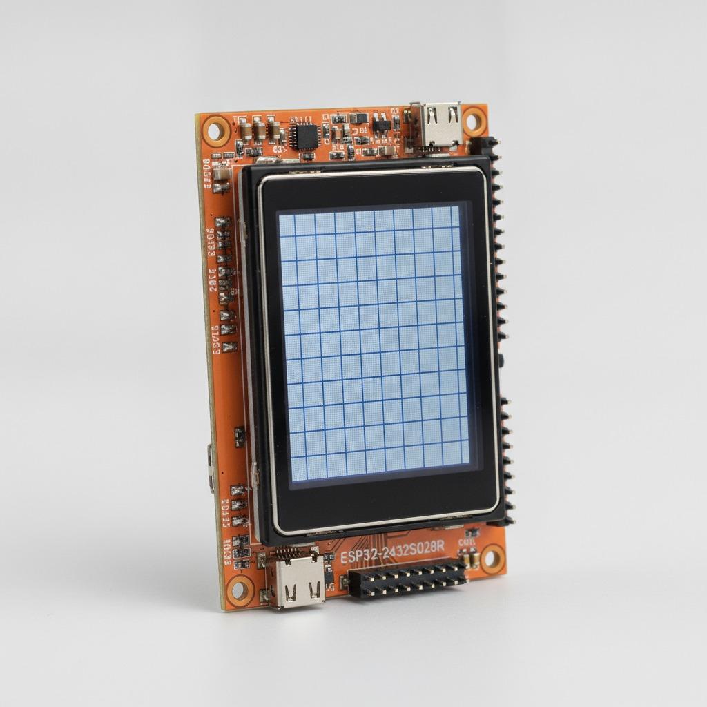
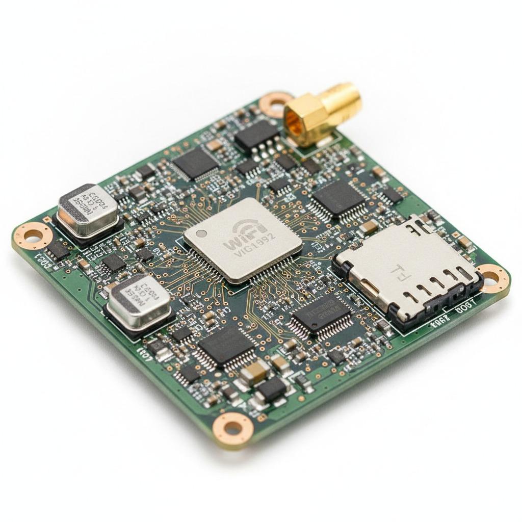
In our daily lives, we are surrounded by a symphony of electronic devices, from the smartphones in our pockets to the complex control systems in our cars. At the core of each of these technological marvels lies a meticulously crafted component: the Printed Circuit Board Assembly, or PCBA. The intricate process of PCBA board manufacturing is what breathes life into these devices, transforming a simple inert board into a functional electronic brain. It is a fusion of precision engineering, advanced robotics, and detailed chemical processes, all working in harmony to create the circuits that power our world. Without this foundational manufacturing process, the digital age as we know it would simply not exist.
From Bare Board to Electronic Blueprint
Before any assembly can begin, there must be a foundation, and in this world, that is the bare Printed Circuit Board (PCB). Imagine a multi-layered sandwich of non-conductive substrate materials, like the common fiberglass composite FR-4, laminated with thin sheets of copper. This copper is then etched away with incredible precision, leaving a delicate network of pathways, or traces, that will act as the wiring for the entire circuit. Over this copper map, a protective solder mask is applied, typically in a vibrant green, blue, or red hue, which insulates the traces and prevents solder from bridging between connections. Finally, a silkscreen layer is printed onto the board, providing a human-readable guide with labels for each component's location. This board is the blank canvas, a detailed blueprint awaiting the electronic components that will give it purpose.
The Art of Component Placement and Soldering
With the blueprint ready, the assembly process commences. The first step involves applying solder paste to the designated component pads on the board. This isn't just a simple application of glue; it is a highly controlled process. A thin, stainless steel stencil, with laser-cut apertures corresponding to every pad, is placed over the PCB. A squeegee blade then glides across the stencil, depositing a precise, uniform layer of solder paste—a grey, metallic substance composed of tiny solder spheres suspended in flux. The accuracy of this single step is paramount, as too little paste can result in a weak connection, while too much can cause shorts, bridging the tiny gaps between components.
Precision Automation and Thermal Fusion
Once the solder paste is applied, the board moves to one of the most visually impressive stages in the entire PCBA board manufacturing journey: automated component placement. Here, high-speed pick-and-place machines, operating with blinding speed and robotic precision, populate the board. These machines use cameras and vacuum nozzles to pick up individual components—from minuscule resistors to complex integrated circuits—from reels and trays, and place them onto their designated pads on the board, pressing them gently into the solder paste. After the board is fully populated, it embarks on a journey through a long reflow oven. The board travels on a conveyor belt through several zones, each with a carefully controlled temperature profile. The heat gradually activates the flux in the paste and then melts the solder, which flows and solidifies to create strong, permanent electrical and mechanical connections. For larger, more robust components, a process called through-hole technology may be used, where component leads are inserted through holes in the board and soldered from the opposite side, often using a wave soldering machine.
Ensuring Perfection: Inspection and Testing
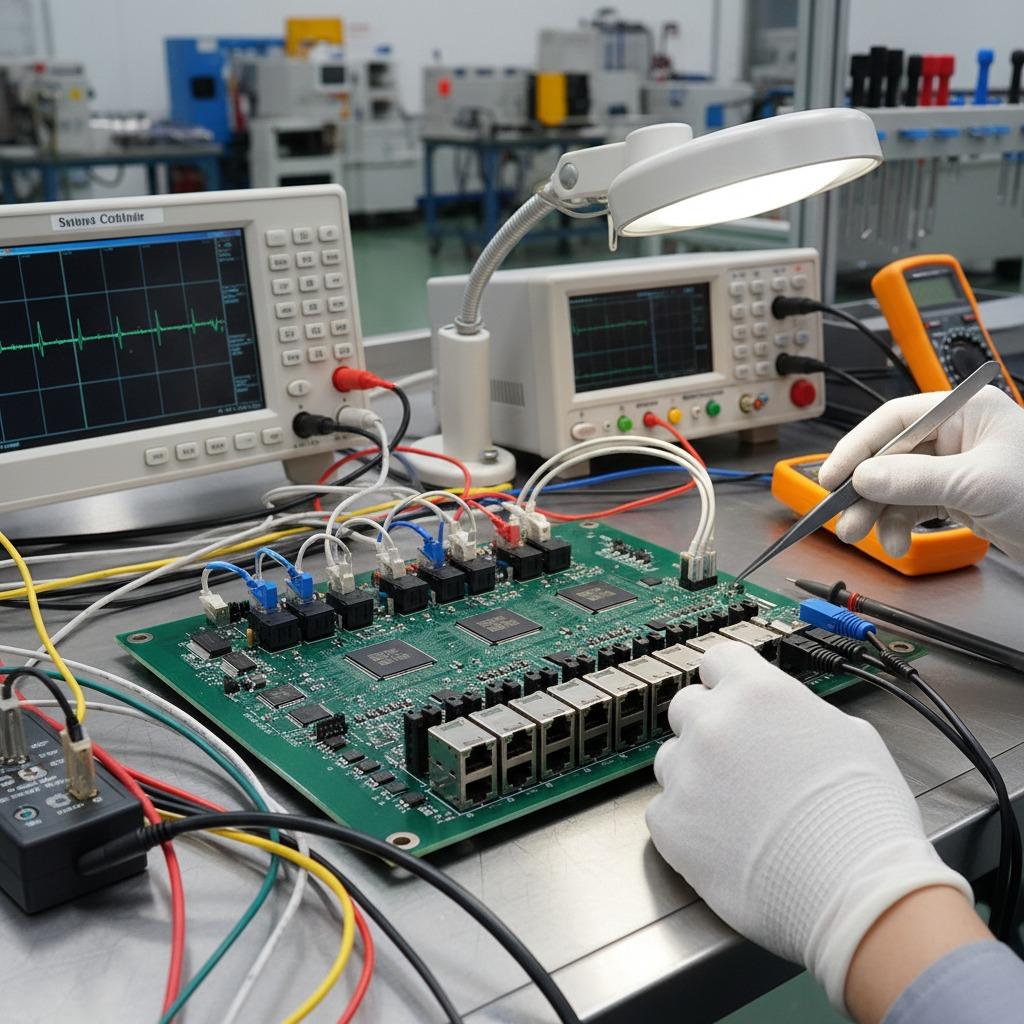
Creating the board is only half the battle; verifying its perfection is just as critical. Following the reflow process, every single board undergoes rigorous inspection. Automated Optical Inspection (AOI) machines use high-resolution cameras to scan the board, comparing it to a flawless reference design to catch any manufacturing defects like missing components, incorrect polarity, or solder bridging. For components with connections hidden underneath the chip, like Ball Grid Arrays (BGAs), X-ray inspection is used to see through the component and ensure all solder balls have connected properly. The final, and most important, stage is functional testing. The board is powered up and its performance is tested to ensure it operates exactly as designed. This commitment to quality control is a non-negotiable cornerstone of the PCBA board manufacturing discipline, guaranteeing the reliability and longevity of the final electronic product.