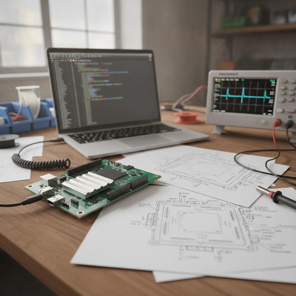
Most PCB issues do not originate in production—they are designed in.
In real projects, teams often discover problems only after prototypes return: signal ringing that was not visible in simulation, MOSFET temperatures rising 20–30°C higher than expected, or boards that pass functional tests but fail EMC certification. By that stage, redesign costs are no longer just engineering time—they affect schedule, tooling, and even certification timelines.
This is where a structured PCB layout service changes the outcome. Instead of treating layout as a final step, experienced teams treat it as a control layer that links electrical intent with real-world constraints. By combining signal integrity rules, thermal behavior modeling, and DFM constraints early, layout decisions become predictable rather than reactive.
What Actually Defines a “Good” PCB Layout in Practice
In theory, layout is about routing and placement. In practice, it is about managing trade-offs.
For example, in a 4-layer board handling both control signals and switching power, placing high-speed traces too close to power loops can introduce noise that only appears under load. Similarly, placing a heat-generating component like a regulator without considering copper distribution can create localized hotspots that shorten lifespan.
A mature PCB layout service does not optimize one parameter at a time. It balances:
-
Signal return paths
-
Power distribution stability
-
Thermal spreading efficiency
-
Assembly feasibility
Projects that follow this integrated approach typically reduce post-prototype redesign cycles by 25–40%, especially in mixed-signal or power-related designs.
Material and Stack-Up Decisions Are Not Just “Specifications”
Material selection is often treated as a checkbox—FR-4 vs high-Tg—but in reality, it directly affects performance drift over time.
In power or automotive-related boards, using standard FR-4 (Tg ~135°C) in high thermal environments often leads to gradual degradation. Switching to high-Tg material (≥170°C) does not immediately change performance, but over 6–12 months of operation, it significantly reduces delamination and parameter drift.
Similarly, stack-up decisions influence both signal integrity and EMI behavior. For example:
-
A poorly defined reference plane can increase impedance fluctuation by 10–15%
-
Lack of continuous ground return paths can increase EMI emissions beyond certification limits
In professional PCB layout service workflows, stack-up is defined together with routing strategy—not afterward—ensuring electrical behavior remains stable across production.
Different Products Require Fundamentally Different Layout Logic
One of the most common mistakes in layout is reusing the same design approach across different product types.
A compact IoT device, for instance, prioritizes space efficiency and antenna isolation. In contrast, a power board prioritizes current handling and thermal dissipation. Trying to apply the same routing density or via strategy to both often leads to hidden issues.
In real projects:
-
Consumer boards often tolerate higher routing density but require cost control
-
Power boards require wider traces (often ≥2–3 mm for high current paths) and thermal relief design
-
Automotive boards emphasize spacing, redundancy, and mechanical stability
A capable PCB layout service adapts layout strategy based on actual operating conditions rather than design convenience.
Environmental Factors Often Define Layout Success
Boards rarely operate in ideal lab conditions. Heat, humidity, vibration, and electrical noise all influence performance over time.
For example, in high-humidity environments, insufficient spacing or poor coating preparation can lead to leakage currents. In vibration-heavy environments, components placed without mechanical consideration can develop solder fatigue.
When environmental adaptation is built into layout:
-
Thermal hotspots can be reduced by redistributing copper and component spacing
-
Failure rates in stress testing typically decrease by 15–30%
-
Long-term stability improves without changing the schematic
These adjustments are rarely visible in design files but are critical in real-world deployment.
How Layout Decisions Translate Into Manufacturing Yield
Layout directly affects whether a design can be produced consistently.
Boards with tight spacing, unnecessary via complexity, or poorly aligned component placement often lead to:
-
Solder bridging
-
Placement misalignment
-
Increased inspection failures
In optimized layouts, aligning design with manufacturing capability leads to measurable improvements.
Layout vs Production Impact (Real Reference Data)
| Layout Decision | Practical Adjustment | Typical Result |
|---|---|---|
| Trace spacing | Match fab capability (≥4–6 mil) | 20–30% fewer shorts |
| Via structure | Reduce unnecessary vias | 8–12% lower drilling cost |
| Component clearance | Improve placement spacing | 15–25% fewer assembly defects |
| Copper balance | Even heat distribution | Lower thermal stress |
| Panel design | Standardized layout blocks | Faster production cycles |
This is where PCB layout service directly influences cost—not by reducing price, but by reducing waste and instability.
Compliance and Safety Begin at Layout Stage
Certification failures are often traced back to layout, not components.
For example:
-
Inadequate creepage distance can fail safety standards
-
Poor grounding can cause EMC test failures
-
Thermal imbalance can violate reliability expectations
Designs aligned with certification requirements from the layout stage significantly reduce rework risk.
A structured PCB layout service ensures that:
-
CE / FCC EMI requirements are considered during routing
-
Clearance and isolation are built into layout
-
Thermal constraints align with reliability expectations
This reduces the likelihood of redesign during compliance testing.
Frequently Asked Questions
Q1: Why do boards pass simulation but fail in real testing?
Because simulation often does not fully capture thermal coupling, EMI interaction, and manufacturing variation.
Q2: Can layout alone improve yield?
Yes. In many cases, layout optimization reduces defects more effectively than process changes.
Q3: Is PCB layout more important than component selection?
Both matter, but layout determines how components actually behave in real conditions.
Why PCB Layout Is the Earliest Point of Control
A well-executed PCB layout service turns design intent into predictable production results. It ensures that signal behavior, thermal performance, and manufacturability are aligned before a single board is built. When layout is treated as a strategic step rather than a finishing task, projects move faster, scale more smoothly, and avoid costly redesign cycles.
If you want to evaluate whether your current design approach can support stable production and long-term performance, reviewing layout methodology and manufacturability alignment is a practical starting point. You can explore our PCB and PCBA capabilities here:
👉 https://www.hcdpcba.com
For projects involving high-speed signals, power density, or complex operating environments, early discussion often prevents late-stage issues. You are welcome to connect with our engineering team here:
👉 https://www.hcdpcba.com/en/contact-us