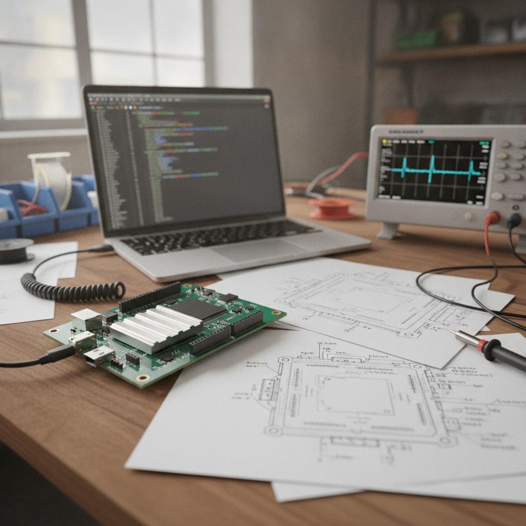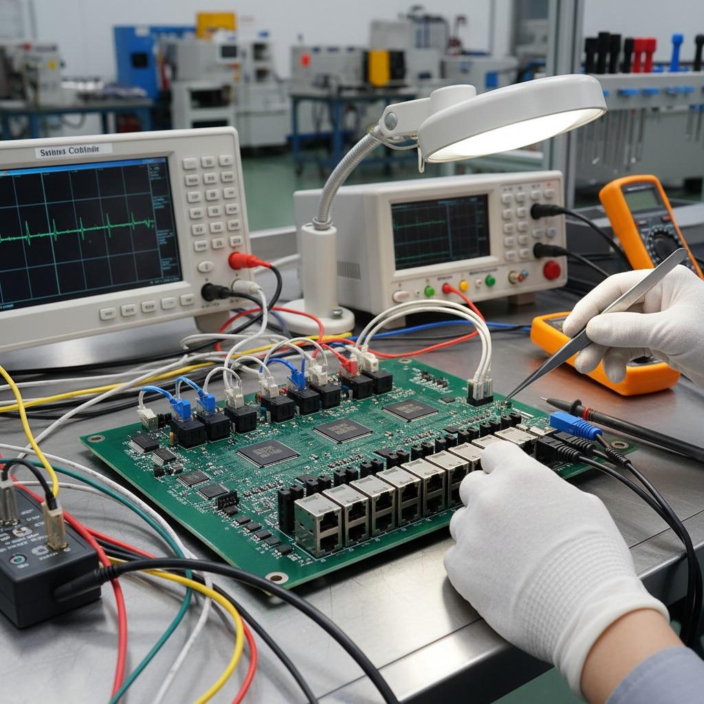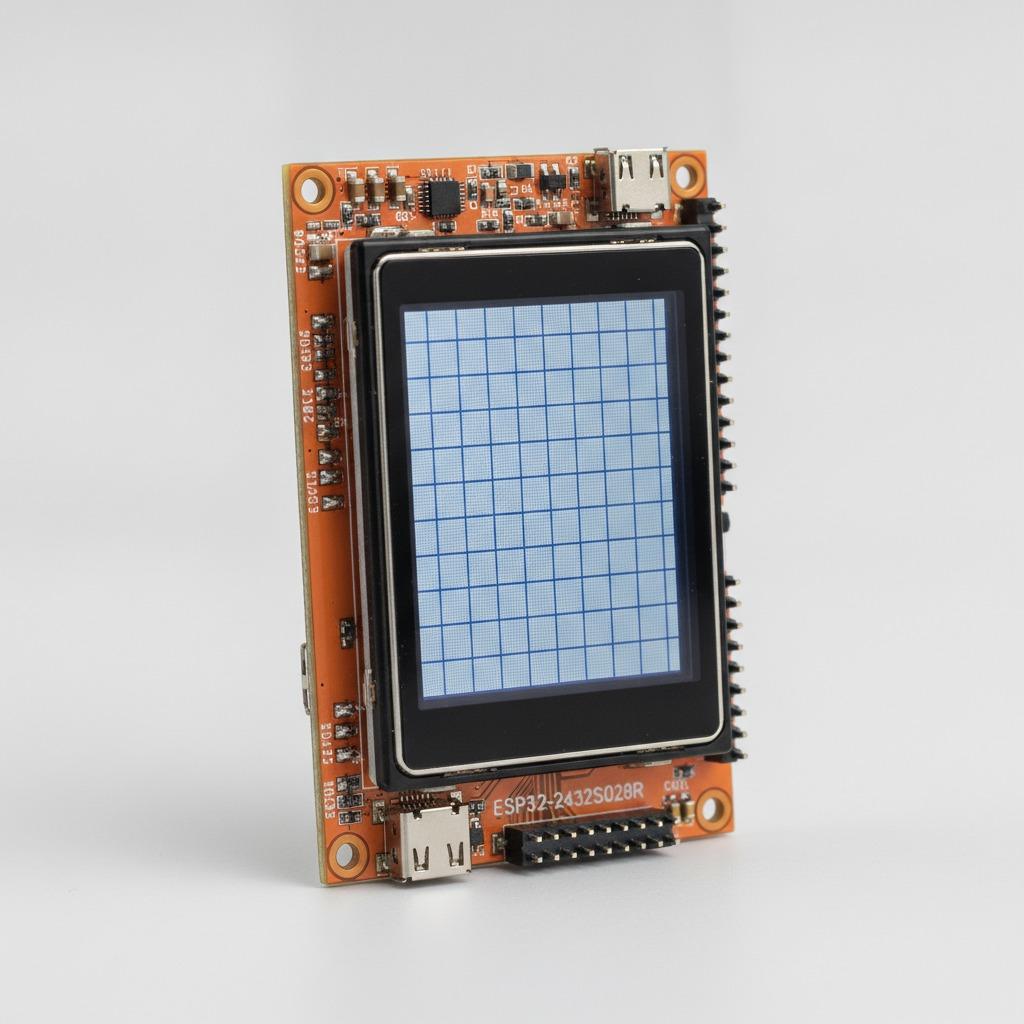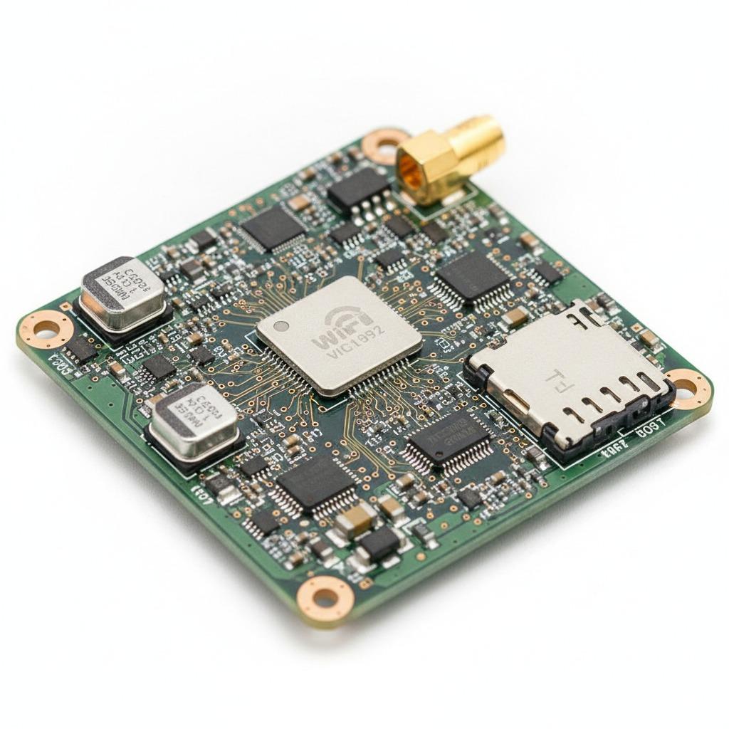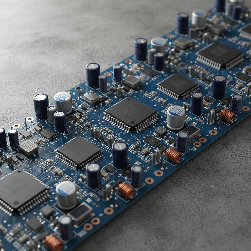
AI devices process enormous volumes of data in real time. Whether the system is handling edge vision processing, neural inference, or machine learning acceleration, the hardware must sustain constant high-speed communication between processors, memory, and peripheral modules.
However, many AI hardware teams discover that early prototypes behave differently once workloads increase. Signal instability, intermittent communication errors, and unexpected latency spikes often appear when data bandwidth reaches its operational limit. These problems are rarely caused by the processor itself. More often, they originate from board-level design decisions that were made without fully considering high-speed routing behavior.
A well-structured high-speed data AI PCBA addresses these challenges by aligning signal routing, stack-up configuration, and manufacturing precision with the actual bandwidth requirements of AI systems. Through optimized impedance control, controlled layer separation, and accurate assembly processes, our engineering team ensures that data pathways remain stable even under sustained computational load.
Why High-Speed Data Architecture Changes PCBA Requirements
Traditional embedded electronics often operate with moderate data rates where small routing imperfections have limited impact. AI systems operate differently. Modern AI boards frequently integrate interfaces such as DDR memory channels, PCIe connections, and high-speed camera or sensor links. These signals travel at several gigabits per second, which means trace geometry and routing symmetry become critical.
In this environment, even small inconsistencies can introduce signal reflection or timing mismatch. For example, a length difference of only a few millimeters between differential pairs may cause skew that disrupts data alignment. Over time, this instability manifests as intermittent errors that are difficult to reproduce during basic testing.
A reliable high-speed data AI PCBA therefore emphasizes strict routing discipline. Controlled impedance traces, carefully matched differential pairs, and properly referenced ground planes ensure that signals propagate predictably across the board.
Engineering teams implementing these practices often observe measurable improvements in communication stability, with signal integrity margins increasing by 15–20% compared with conventional routing approaches.
Material and Stack-Up Choices for High-Speed AI Boards
Signal performance is not determined solely by routing geometry. PCB material and stack-up structure also influence data integrity, particularly when signal frequencies rise above several gigahertz.
Standard FR-4 materials may perform adequately for moderate-speed electronics, but high-speed AI systems often benefit from low-loss laminates. Materials with a dielectric loss factor (Df) below 0.005 significantly reduce signal attenuation, allowing long high-speed traces to maintain clean waveforms.
Stack-up planning is equally important. Multi-layer structures—commonly ranging from six to twelve layers—allow designers to separate signal layers from power and ground planes. This separation stabilizes impedance and reduces electromagnetic interference between adjacent traces.
When a high-speed data AI PCBA integrates optimized materials and stack-up architecture, systems often achieve both improved signal clarity and better EMI control, reducing the likelihood of redesign during system integration.
Power Density and Thermal Management in AI Processing Boards
AI processors and accelerators consume considerable power during computation bursts. When combined with high-speed memory modules and communication interfaces, power density increases rapidly in a limited physical area.
Without proper thermal planning, heat generated by these components can accumulate around processing clusters. Elevated temperatures degrade semiconductor efficiency and may cause throttling in AI devices designed for continuous workloads.
In practical board designs, thermal control involves more than simply adding heat sinks. Copper distribution across internal layers spreads heat laterally, while arrays of thermal vias help transfer energy away from critical components.
A well-designed high-speed data AI PCBA integrates these thermal strategies directly into the layout stage. Systems that employ balanced copper structures and optimized component placement often reduce peak hotspot temperatures by 10–25°C, significantly improving long-term operational stability.
Manufacturing Precision and Data Reliability
High-speed signal performance can degrade if assembly tolerances vary between production batches. Slight differences in solder thickness or component alignment can subtly change impedance characteristics and introduce signal irregularities.
Manufacturing discipline therefore becomes a critical factor for AI hardware production. Stable stencil design, accurate placement calibration, and consistent reflow temperature profiles ensure that every board maintains the same electrical behavior.
Manufacturing Factors Affecting High-Speed AI PCBA
| Manufacturing Factor | Control Method | Typical Result |
|---|---|---|
| Differential pair routing | Length matching | Reduced signal skew |
| Impedance control | Controlled stack-up | 15–20% signal integrity improvement |
| Thermal copper balancing | Even heat distribution | Lower hotspot formation |
| Placement accuracy | Fine-pitch alignment | Improved signal reliability |
| Process stability | Controlled reflow profile | Reduced batch variation |
Through these controls, a production-ready high-speed data AI PCBA maintains consistent performance even as manufacturing volume increases.
Compliance and Reliability in AI Hardware Platforms
AI devices deployed in commercial or industrial environments must also meet regulatory requirements related to electromagnetic compatibility and electrical safety. High-speed signals generate switching noise that can easily exceed regulatory emission limits if layout and grounding strategies are poorly designed.
Proper layer isolation, grounding schemes, and signal shielding techniques help control electromagnetic radiation while maintaining signal quality. Designing these requirements directly into the PCBA stage minimizes certification risk and reduces costly redesign cycles.
Frequently Asked Questions
Q1: Why do AI boards experience data instability under heavy load?
Because high-speed signals become sensitive to routing imbalance and impedance variation when bandwidth increases.
Q2: Does PCB material significantly affect AI performance?
Yes. Low-loss materials help preserve signal quality across long high-speed traces.
Q3: Can manufacturing variation influence AI system behavior?
Absolutely. Even small assembly deviations can affect impedance consistency and signal timing.
Why High-Speed Data Design Defines AI Hardware Reliability
The performance of AI hardware depends not only on processors or algorithms but also on how efficiently data moves across the board. A carefully engineered high-speed data AI PCBA ensures that signal integrity, power stability, and thermal balance remain consistent as computing workloads scale.
If you want to understand how board-level architecture affects AI system reliability and manufacturing scalability, exploring proven PCBA capabilities is an effective starting point. You can learn more about our manufacturing experience and engineering approach by visiting our official website:
👉 https://www.hcdpcba.com
For projects involving high-speed interfaces, AI computing modules, or data-intensive devices, discussing your specific requirements early can significantly reduce development risk. Our engineering team is available for technical consultation here:
👉 https://www.hcdpcba.com/en/contact-us