AI Device PCBA Factory: Where Intelli gent Hardware Becomes Deployable at Scale
AI hardware is no longer confined to labs or proof-of-concept demonstrations.
Today, AI-enabled devices operate continuously in factories, retail spaces, transport systems, and distributed edge environments. They analyze images, process audio, make decisions, and communicate with cloud platforms—often under sustained load and limited thermal margin.
This shift fundamentally changes what an AI device PCBA factory is expected to deliver.
It is not enough to assemble a complex board once. The real challenge is producing PCBAs that behave consistently under real workloads, across hundreds or thousands of units, without gradual performance drift.
At this level, PCBA manufacturing becomes a foundation for system reliability, not a downstream task.
AI Device PCBAs: Why Manufacturing Tolerance Matters More Than Ever
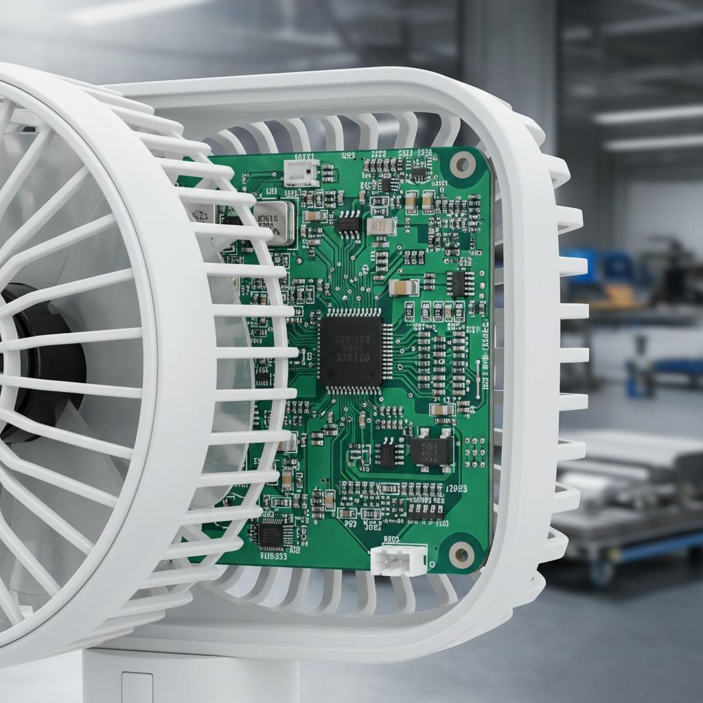
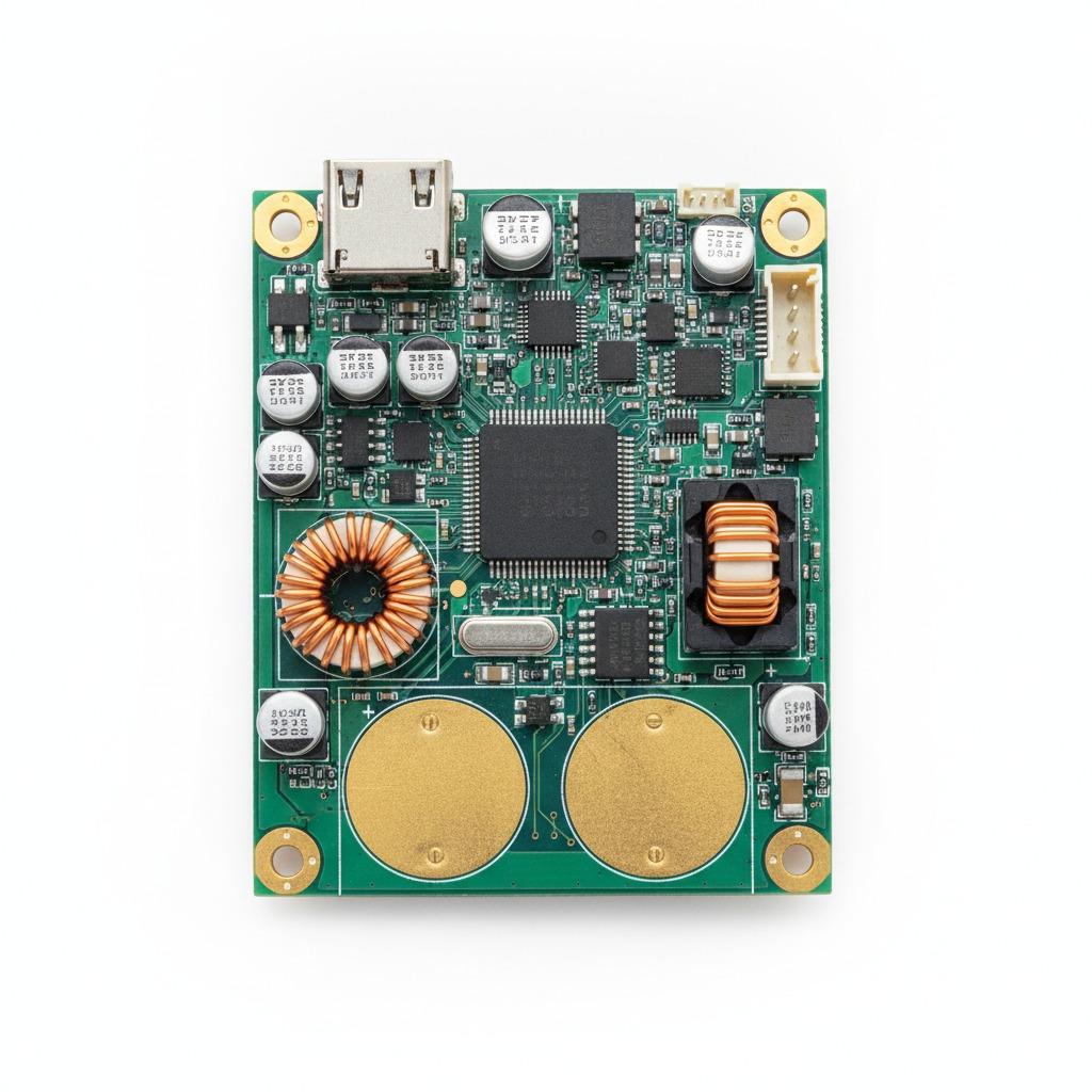
AI device PCBAs differ from traditional control boards in one critical way: they are workload-driven.
Processors, memory, and accelerators operate together at high utilization, drawing dynamic current and generating continuous heat. Small variations introduced during assembly—slightly uneven solder joints, marginal power paths, inconsistent thermal contact—can translate into instability once devices run inference workloads for hours or days.
This is why AI-focused PCBA production places far more emphasis on consistency than on speed alone. Assembly processes must ensure that what works in the first batch behaves the same way in later builds, even as volumes increase.
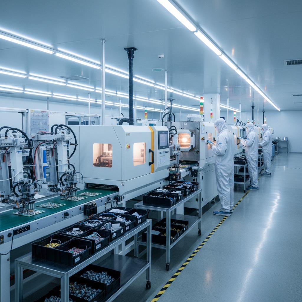
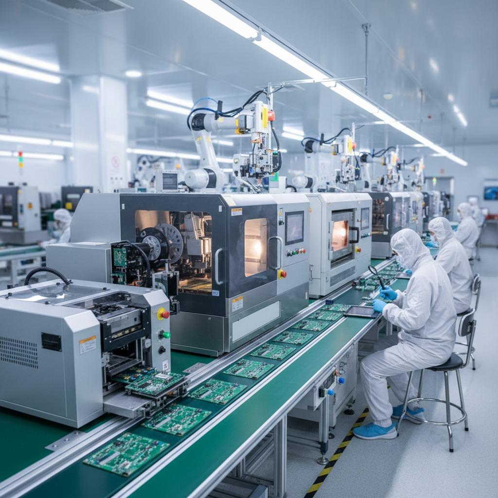
Manufacturing Discipline Behind High-Density AI Assemblies
From the outside, AI PCBAs look similar to other dense electronic boards. The difference appears during assembly.
High-pin-count processors, tightly packed memory, and layered power planes reduce tolerance for variation. Reflow behavior, solder volume control, and placement accuracy must all be tightly aligned with board structure and component mix.
In practice, an AI device PCBA factory pays particular attention to:
-
Uniform solder joint formation on dense pads
-
Stable placement of large compute components
-
Controlled thermal exposure during reflow
-
Verification of hidden joints where visual access is limited
These steps are not about achieving theoretical perfection. They are about ensuring predictable behavior under sustained compute load, which is where AI devices truly get tested.
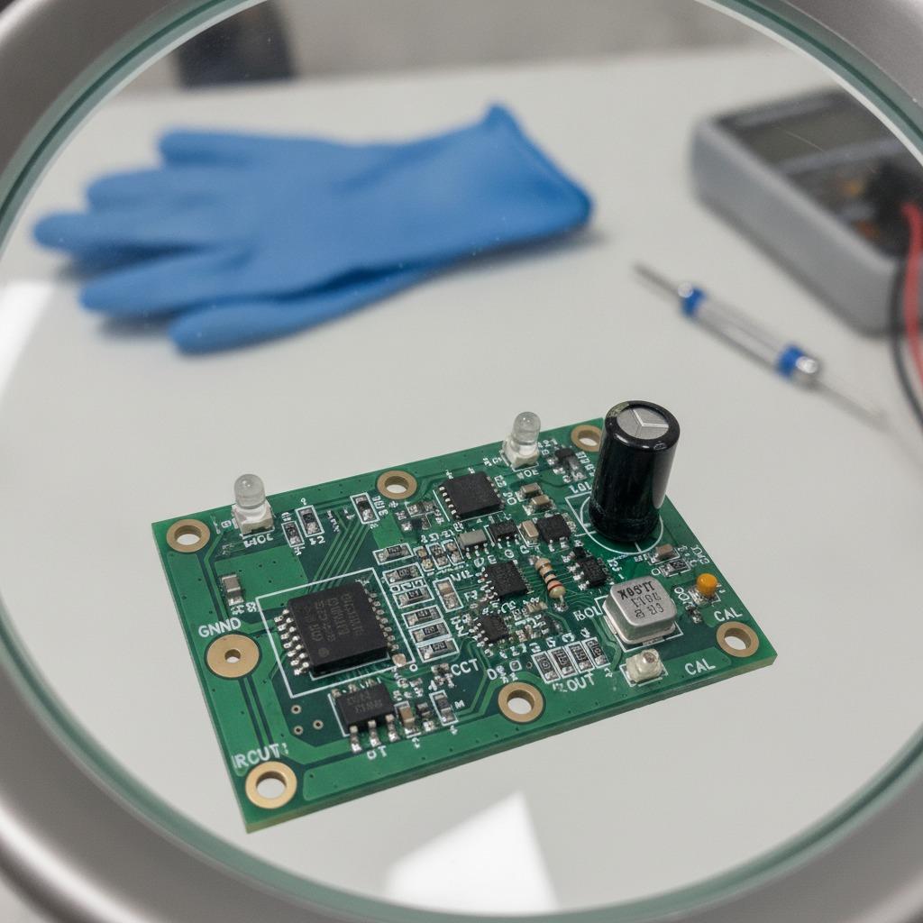
Power Delivery and Thermal Behavior Under Real AI Workloads
AI devices rarely fail because a component is missing.
They fail when power delivery becomes unstable or when heat accumulates unevenly over time.
During PCBA production, power-related assembly quality has a direct impact on how voltage rails behave under load. Inconsistent joints on regulators, inductors, or high-current paths can introduce localized resistance, which then manifests as heat concentration during operation.
An experienced AI device PCBA factory accounts for this by aligning assembly practices with power and thermal intent:
-
Power components are mounted with consistent joint geometry
-
High-current paths are assembled to minimize resistance variation
-
Mechanical stability is maintained to prevent joint fatigue during thermal cycling
-
Assembly remains compatible with downstream heat spreaders or cooling structures
When these factors are controlled at the PCBA stage, system-level thermal design becomes far more effective.
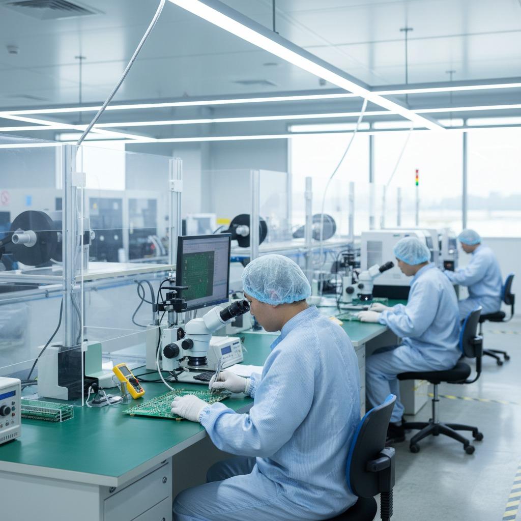
Testing AI PCBAs Under Conditions That Reflect Real Use
Basic electrical testing confirms that a board powers on.
For AI devices, that is only the starting point.
Because AI workloads stress both power delivery and thermal paths, testing must extend beyond simple continuity checks. AI-focused PCBA factories validate behavior under conditions that resemble actual use, even during early production stages.
AI Device PCBA Testing Focus
| Test Focus | Why It Matters for AI Devices |
|---|---|
| AOI & X-ray | Confirms dense and hidden joints are consistent |
| Electrical testing | Verifies stability of multiple power domains |
| Functional testing | Confirms AI modules boot and operate correctly |
| Thermal observation | Identifies heat concentration during load |
| Burn-in testing | Reveals early drift under sustained operation |
This approach helps catch issues that only appear after prolonged computation, long before devices reach deployment.
From Pilot Builds to Volume Deployment
Most AI products do not begin with mass production. They start with pilot runs—dozens or hundreds of units used for validation, customer trials, or limited deployment.
A capable AI device PCBA factory ensures that these early builds are production-representative, not laboratory exceptions. Assembly parameters, sourcing strategy, and inspection logic remain consistent so that scaling does not introduce new variables.
This continuity reduces the risk of redesigns, late-stage adjustments, or unexpected yield loss when volumes increase.
Where AI Device PCBAs Are Commonly Used
AI PCBA manufacturing supports a broad range of intelligent hardware applications. These devices differ in form factor and function, but share common demands on stability and consistency.
Typical application areas include:
-
Vision-based AI cameras and analytics devices
-
Industrial inspection and automation platforms
-
Smart retail and access control systems
-
Robotics and autonomous equipment
-
Embedded AI gateways and controllers
Each scenario introduces different stress profiles, which the PCBA process must handle without compromise.
Frequently Asked Questions
Q: Can AI device PCBAs be produced using standard consumer electronics assembly lines?
A:Standard lines may assemble the boards successfully, but they often lack the process discipline needed for sustained AI workloads. Without tighter control over power-related assembly and thermal behavior, long-term stability can be compromised.
Q: How early should PCBA manufacturing considerations be included in AI hardware projects?
A:Ideally at the prototype stage. When pilot builds follow production-aligned processes, scaling becomes smoother and fewer surprises appear during volume deployment.
Q: What is the biggest manufacturing risk specific to AI device PCBAs?
A:Inconsistent behavior under load. AI devices may pass basic tests but fail after prolonged operation if power delivery or thermal paths are marginally assembled.
Reliable AI Hardware Starts With the Right PCBA Foundation
AI devices succeed or fail based on how consistently they operate under real workloads.
A professional AI device PCBA factory provides the manufacturing discipline needed to translate complex AI designs into scalable, reliable hardware platforms.
To discuss AI device PCBA requirements or production support, visit www.hcdpcba.com or contact the team directly via:
https://www.hcdpcba.com/contact-us