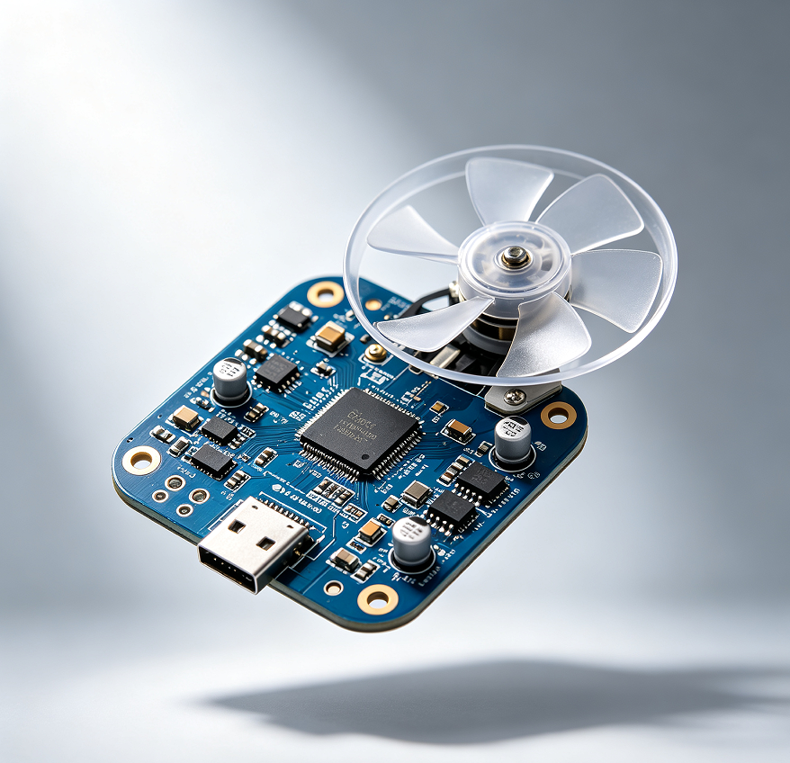
In the fast-paced world of modern electronics, RF Communication PCB Assembly stands out as a cornerstone technology for seamless connectivity and high-performance devices. At hcdpcba, we specialize in delivering precision-engineered RF Communication PCB Assembly solutions that empower innovators to bring their visions to life. This advanced assembly process integrates radio frequency components with meticulous craftsmanship, ensuring reliable signal transmission in compact gadgets. Imagine a miniaturized electronics board that fits effortlessly into wearables or smart home devices, buzzing with potential thanks to its integrated circuits, capacitors, and strategic button placements for intuitive user interaction.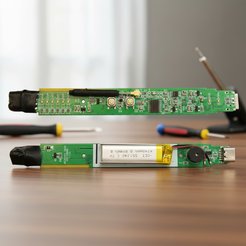
Delving deeper into our RF Communication PCB Assembly expertise, we craft boards that excel in RF Signal Processing PCB applications. These boards handle complex signal modulation and amplification with unparalleled efficiency, making them ideal for telecommunications and IoT ecosystems. Our top-view designs reveal a symphony of components working in harmony—integrated circuits pulsing with data, capacitors storing energy for swift responses, and buttons that invite user engagement. Flipping to the bottom, a rechargeable lithium-ion battery ensures uninterrupted power, while the micro USB port facilitates effortless charging and data transfer. This isn't just assembly; it's a fusion of form and function, where every solder joint and trace is optimized for RF integrity, minimizing interference and maximizing range in devices like wireless sensors or portable communicators.
For those venturing into specialized realms, our PCB Assembly for RF Applications takes innovation to new heights. hcdpcba's comprehensive services, including SMT placement and PCBA customization, support multi-layer HDI and high-frequency boards tailored for industries such as automotive electronics, medical devices, and smart grids. Picture a board where a small buzzer delivers crisp audio alerts, enhancing user experience in security systems or health monitors. We go beyond standard assembly by offering component sourcing, rigorous testing, and DFMA analysis to streamline production and cut costs without sacrificing quality. Our experienced team ensures zero-defect outcomes, backed by rapid prototyping and OEM/ODM support that aligns with your unique needs.
What sets hcdpcba's RF Communication PCB Assembly apart is our commitment to versatility and reliability across diverse applications. From powering AI-driven smart homes to enabling secure communications in industrial controls, our RF Signal Processing PCB solutions deliver vivid performance in every scenario. Clients in telecommunications and beyond trust our swift response times, cost-effective processes, and stringent confidentiality measures. Whether you're prototyping a groundbreaking wearable or scaling production for mass-market gadgets, our PCB Assembly for RF Applications provides the robust foundation needed for success. With over a decade of expertise, we invite you to explore how our miniaturized boards can transform your projects—contact us at +86 18924624188 to start your journey toward cutting-edge electronics today.
In essence, RF Communication PCB Assembly at hcdpcba isn't merely a service; it's a gateway to the future of connected technology. Our boards encapsulate advanced engineering in a compact form, blending powerful RF capabilities with user-friendly features like extended battery life and seamless connectivity. As demands for faster, more reliable wireless systems grow, our tailored RF Signal Processing PCB and PCB Assembly for RF Applications ensure your products stay ahead. Join the ranks of satisfied partners in fields like IoT, automotive, and medical tech who rely on our quality-assured, high-frequency solutions to drive innovation and efficiency.
Loading...