In the fast-paced world of portable electronics, the Fast Charging PCB Board stands out as a revolutionary component that powers up devices with unmatched speed and efficiency. At hcdpcba, we pride ourselves on delivering cutting-edge solutions that blend innovation with reliability, and this board is no exception. Designed for seamless integration into modern gadgets, it transforms ordinary power management into a high-performance symphony of circuits and connections. Imagine a compact powerhouse that not only charges batteries swiftly but also ensures safety and longevity, all while fitting snugly into your next project.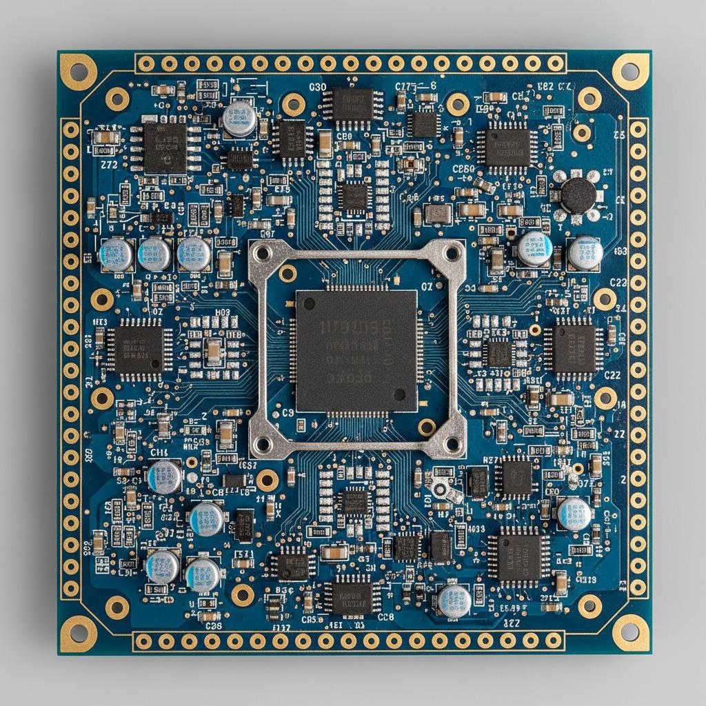
Delving deeper into its architecture, our Fast Charging PCB Board incorporates dual voltage rails that gracefully handle multiple inputs through VBUS01 and VBUS02 connectors, painting a picture of versatile energy flow. Picture the board's surface alive with integrated charging systems, where sophisticated ICs dance alongside capacitors like C5 and C8, and inductors such as L1, orchestrating a ballet of efficient power distribution. This isn't just hardware; it's a meticulously crafted ecosystem that shields against over-voltage threats, particularly in the GATEA and GATEB zones, ensuring your devices remain protected amid rapid charging cycles. For those crafting USB Power Bank PCB designs, this board elevates the game by supporting intelligent data exchange via DM and DP pads, fostering connections that feel almost intuitive. The glow of LED indicators adds a visual narrative, instantly revealing status updates with vibrant, responsive lights enhanced by low-resistance pathways that whisper efficiency.
What truly sets our Compact Power Bank PCB Design apart is the thoughtful fusion of discrete components, where SMD resistors like R14, R16, and R50 mingle with capacitors C19 and C35 in a compact harmony. Envision a layout so optimized that signal routing flows like a river, minimizing interference and amplifying clarity, even in the harshest environments. At hcdpcba, our expertise in SMT贴片 and PCBA板 production shines through, offering not just a board but a gateway to streamlined power management. Whether you're developing for consumer electronics, industrial controls, or the burgeoning fields of IoT and smart homes, this Fast Charging PCB Board adapts effortlessly, backed by our comprehensive services from PCB打样 to full OEM and ODM solutions. Our team's technical prowess ensures every trace and solder joint contributes to a robust, future-proof design that minimizes thermal hotspots and maximizes signal integrity.
Beyond the specs, the allure of this USB Power Bank PCB lies in its real-world impact. Developers can now prototype with confidence, knowing hcdpcba's rapid response and quality assurance—rooted in strict controls and cost-optimized processes—deliver zero-defect results. From sourcing genuine components through our 元器件代采 service to rigorous testing that uncovers every nuance, we handle the complexities so you can focus on innovation. In applications spanning medical devices, automotive electronics, and AI-driven systems, the Compact Power Bank PCB Design proves its mettle by enabling faster charge times without compromising on safety or size. It's more than a circuit board; it's the heartbeat of portable power, inviting engineers to build brighter, more connected futures. With hcdpcba's commitment to confidentiality and personalized support, partnering with us means unlocking potentials you never knew existed in fast charging technology.
As we continue to push boundaries in electronics engineering, the Fast Charging PCB Board embodies hcdpcba's dedication to excellence. Contact us at +86 18924624188 to explore how this innovation can supercharge your projects, complete with DFMA analysis for even greater efficiency. In a world demanding more from less, this board doesn't just charge—it inspires.
Loading...