
Power Bank PCBA Overview
A Power Bank PCBA is the control and power conversion core inside a portable charger. It solves a practical buyer problem: how to pack charging input, battery management, and regulated output into a compact board that can fit a portable enclosure. For OEM and ODM projects, this kind of board is the link between the battery cell, the USB interface, and the end-user charging experience. When the layout, connector choice, and assembly quality are stable, the finished product is easier to integrate and easier to scale.
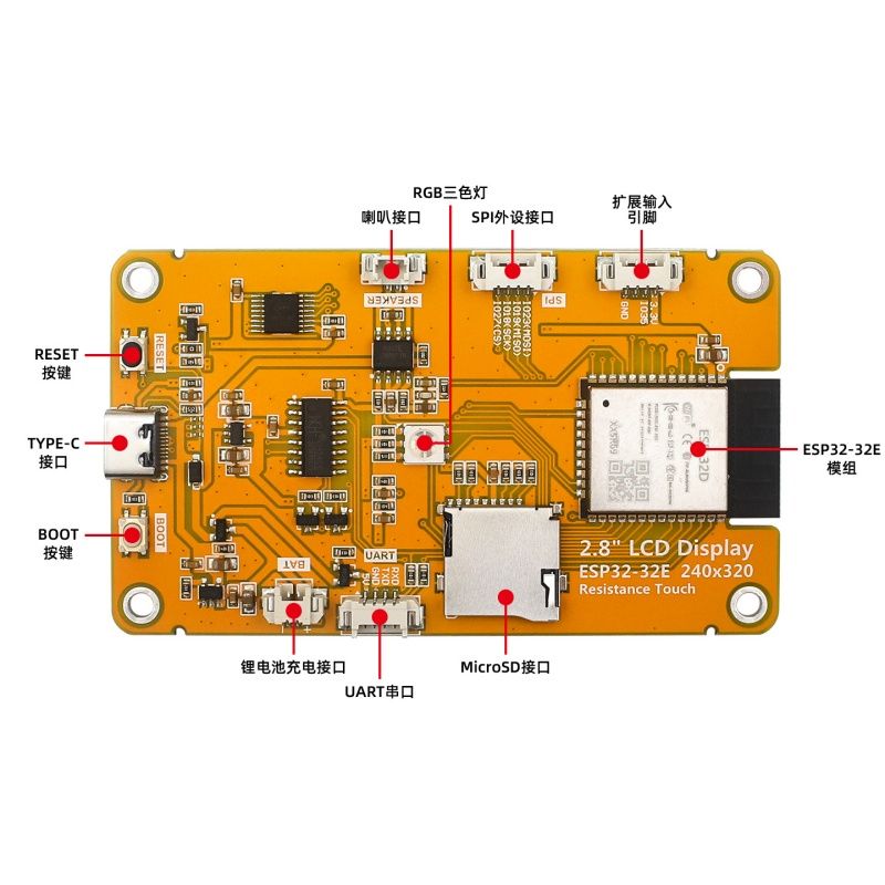
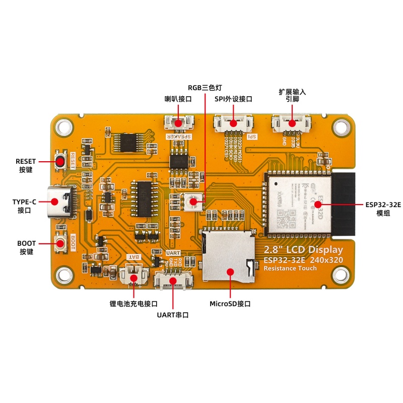
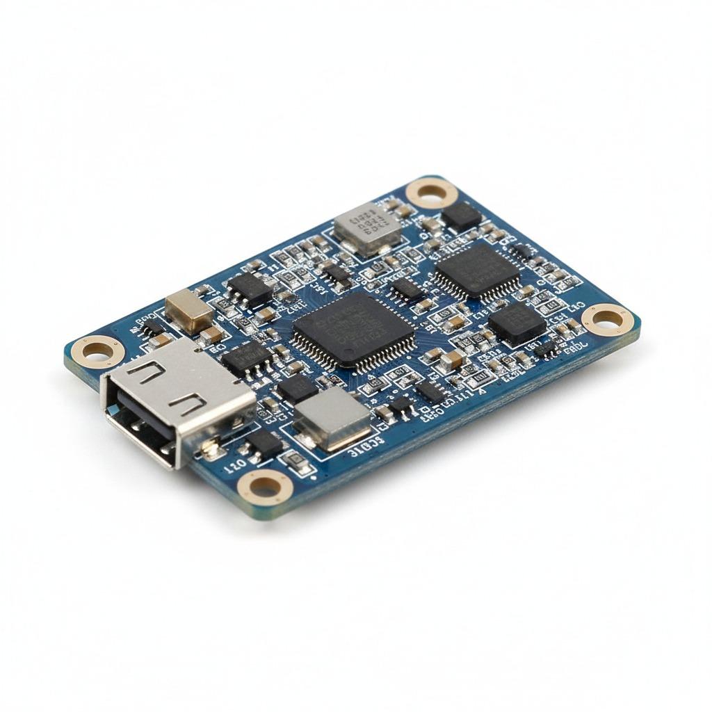
In the visible board examples, the assembly includes a rigid PCB, surface-mount components, mounting holes, and connector interfaces such as USB Type-C. The board marking suggests a PD fast charging function, but exact electrical ratings are not provided, so any performance specification should be confirmed through design documentation and test data.
Product Structure and Functional Positioning
This type of board is commonly used as a Power Bank Motherboard or Mobile Power Supply PCB in portable energy products. Its role is to manage the flow of power between input and output paths, while supporting the control logic required for charging and protection. Depending on the design, it may also coordinate battery status indication, bidirectional charging behavior, and interface communication through Type-C ports.
The visible assemblies show a compact rectangular format with integrated ports, which is useful for handheld devices where board space is limited. Mounting holes near the corners help with enclosure fixing, standoff alignment, and mechanical stability during assembly.
Key Capabilities Buyers Usually Evaluate
Power routing and charging control
A Power Bank Circuit Board Assembly should support clean power routing with minimal assembly variation. Buyers often look at how the board handles input from a charger, internal battery connection, and output to consumer devices.
Type-C interface integration
When a board includes a USB-C port, integration quality matters as much as the connector itself. The PCB footprint, solder joint strength, and nearby component placement affect reliability during repeated plug-in cycles. A Type-C Power Bank PCBA is typically chosen for compact designs that need modern charging connectivity.
Fast-charge architecture
The marking and layout indicate a fast-charge oriented design, which may be suitable for portable charging products that need efficient power delivery. If the project requires Bidirectional Fast Charge PCBA functionality, the buyer should confirm protocol support, electrical limits, thermal design, and battery compatibility before production.
Materials, Board Finish, and Visible Construction
From the image data, the board appears to use a fiberglass-based rigid substrate with solder mask finish. One sample shows a blue solder mask with white silkscreen, while another visible board example has an orange solder mask. Both are common finishes in electronic assemblies and mainly serve to protect the copper and support legible marking. The components are surface-mounted, and the layout includes passive parts, ICs, and a larger central module or power-related package.
Visible connector structures include USB-type interfaces and small board-edge connectors. Because the exact chipset and layer count are not readable, those details should be treated as unknown until confirmed by the design package or BOM.
Manufacturing Process and Assembly Flow
For this category, production usually starts with PCB fabrication, followed by SMT placement and reflow soldering. Depending on the design, through-hole steps, connector soldering, board inspection, and functional testing may also be included. hcdpcba supports PCB fabrication, SMT贴片, component sourcing, assembly, and testing, which is useful for buyers who want one supplier to manage the build from prototype to volume production.
DFMA review is especially valuable for a power board. Small layout changes can affect thermal behavior, connector access, and assembly yield. A good assembly plan should also consider polarity marking, clearance around high-current paths, and the mechanical load applied by external cables.
Typical Application Scenarios
Power bank modules are the most direct use case, but the same assembly logic also applies to portable electronics power management, consumer charging hardware, embedded device integration, and board-level replacement projects. In some projects, a Mobile Power Supply PCB is used as part of a custom enclosure with a battery pack, indicator LEDs, and one or more external ports.
For development teams, this type of board may also be used in prototype platforms where a compact charging and output circuit is needed before final industrial design is frozen.
Quality Control and Buyer Decision Factors
When evaluating a Power Bank PCBA, buyers should focus on process control rather than visual appearance alone. Important decision factors include solder joint consistency, connector alignment, component traceability, test coverage, and the ability to repeat the same build across batches. If the product will be sold under OEM branding, documentation and inspection records are often as important as the board itself.
It is also wise to confirm firmware support, protection functions, battery interface requirements, and any compliance targets that apply to the final market. Since the supplied images do not show exact electrical data, those points should be clarified during quoting.
Customization Options for OEM and ODM Projects
Custom work may include connector selection, port arrangement, board outline changes, silkscreen labeling, component substitution, enclosure-fit adjustments, and test fixture development. For a Power Bank Motherboard, these changes can make the difference between a board that only works on paper and a board that fits smoothly into mass production.
If you need a specific feature set such as Type-C Power Bank PCBA integration, request a design review early. That helps align the PCB layout, mechanical constraints, and assembly process before tooling and pilot builds begin.
Request a Build Review
hcdpcba provides PCB打样, SMT贴片, 元器件代采, 组装, 测试, and OEM/ODM services for custom electronic boards. If you are sourcing a Power Bank PCBA for a portable charger, fast-charge module, or related power electronics project, send your schematic, BOM, Gerber files, or sample board requirements for evaluation. A clear technical review at the start usually saves time in later stages of production.