Mobile Charger PCB Overview
A mobile charger pcb is the electronics heart inside a USB charger or compact power adapter, turning mains AC into stable DC power for phones, earbuds, tablets, and other USB-powered devices. For buyers, the main problem it solves is simple but critical: safe, repeatable charging in a small enclosure without overheating, unstable output, or unreliable assembly. In a retail charger, travel adapter, or custom power module, the board layout and assembly quality often decide whether the product feels solid in daily use or fails early under load.
At hcdpcba, the focus is on practical PCB and PCBA manufacturing for products like chargers, control boards, and embedded modules. Whether the design is for a consumer accessory or an industrial power-related assembly, the board must fit the housing, manage heat, and keep the circuitry consistent from batch to batch.
Product Overview
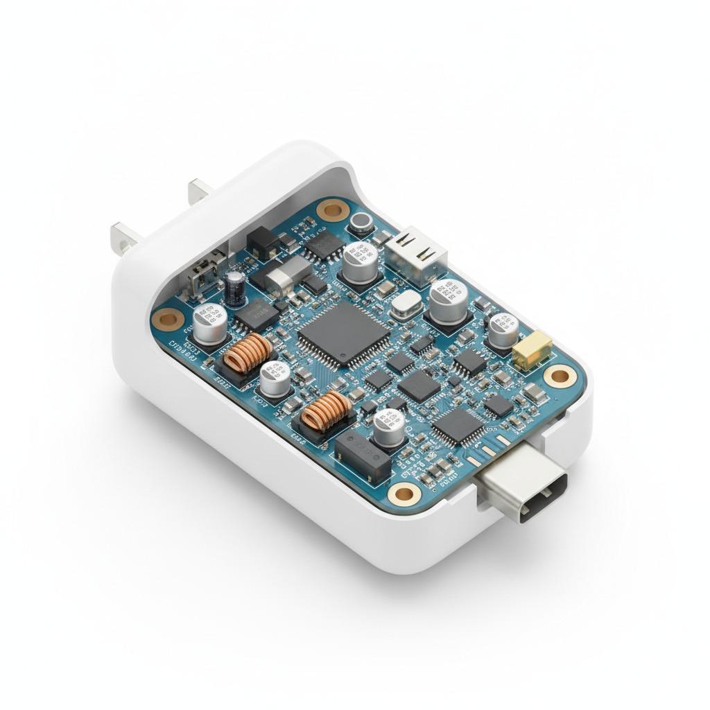
Based on the visible product structures, charger-related PCB assemblies typically combine a compact circuit board, power conversion parts, protective components, and connector interfaces. A USB wall charger format usually needs a dense internal arrangement because the enclosure is small while the electronic function is demanding. The visible examples suggest a mixed environment of surface-mount devices, power-filtering components, and connector-based interfaces, which is common in compact charger and adapter products.
A usb charger circuit board is usually designed around space efficiency. Even when the outer housing looks simple, the internal assembly can include rectification, filtering, control, and output regulation sections. For a buyer, that means the real value is not just the shell but the quality of the board layout, solder joints, and component integration.
Key Specifications and Capabilities
Visible and practical features
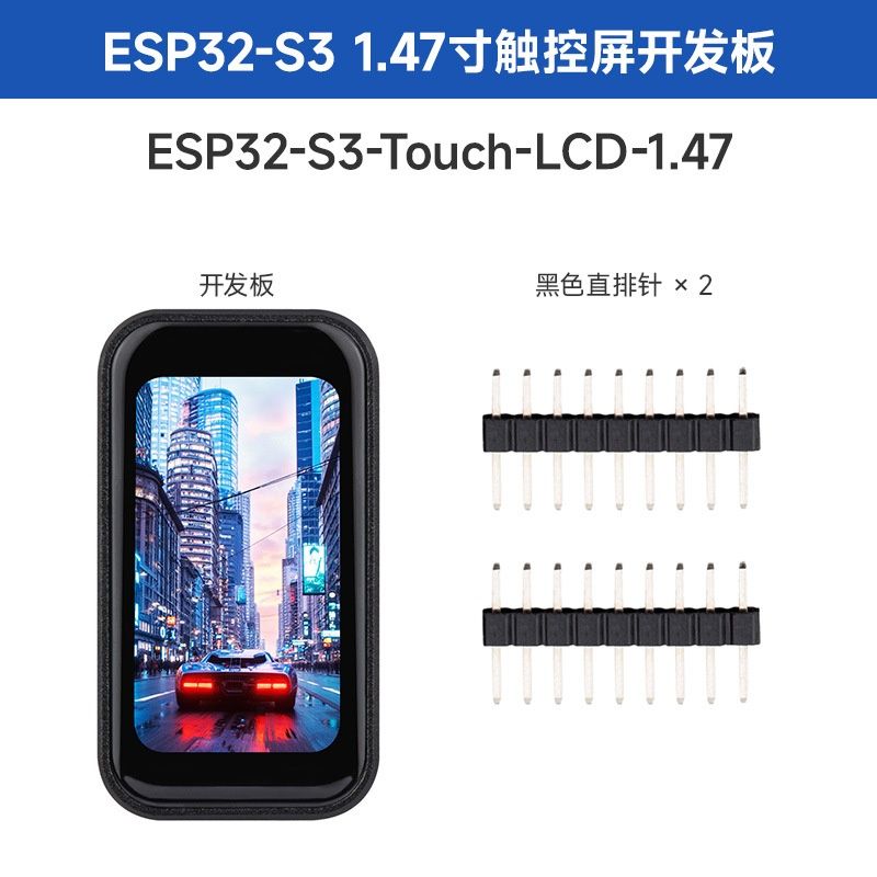
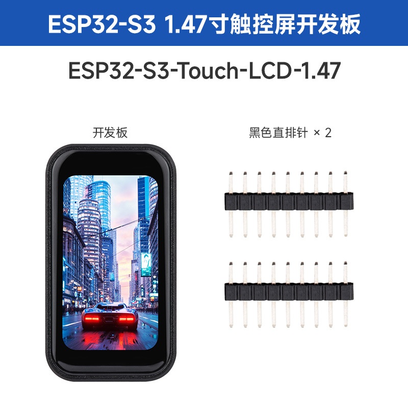
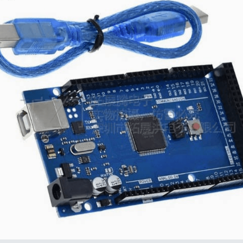
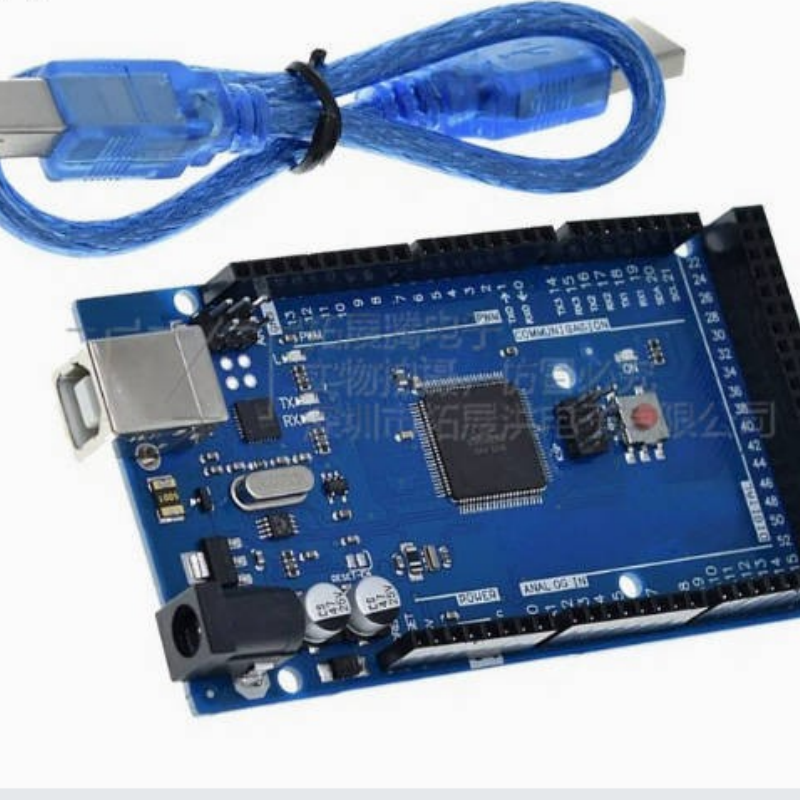
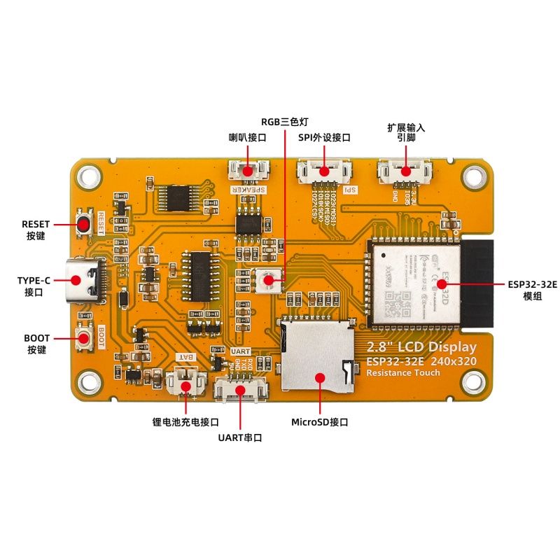
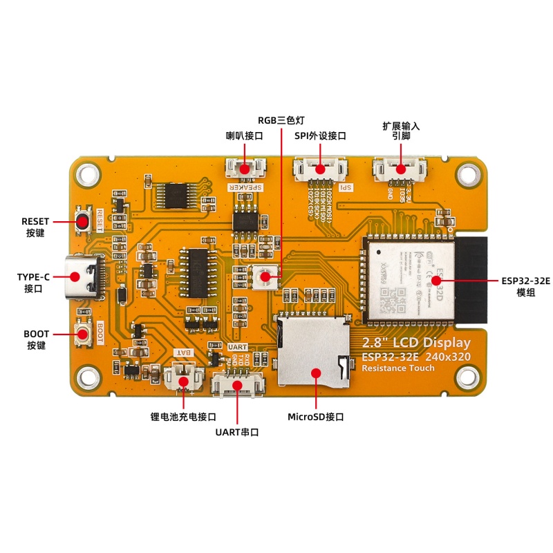
The provided product images and notes show several useful, verifiable characteristics: compact board geometry, dense component placement, fine-pitch IC packages, surface-mounted passives, gold-colored mounting holes, and connector-based interfaces. In the charger-style example, one USB-C output port is visible on a compact wall-plug body. In the PCB assembly examples, there are also edge connectors and mounted components that indicate functional electronic integration rather than a bare substrate.
What buyers usually evaluate
When sourcing a fast charging pcba or standard charger board, buyers normally compare output design, thermal behavior, board size, connector arrangement, component placement, and compatibility with the target enclosure. Exact electrical ratings are not provided here, so those should be confirmed in the design file, BOM, or sample testing. For custom builds, the same physical board can support very different output profiles depending on the circuit design.
Materials and Finish Options
The visible PCB assemblies appear to use standard FR-4-style substrate construction with blue-green solder mask, white silkscreen, copper traces, and plated pads. This is the familiar backbone of many consumer and industrial electronics products. The charger housing shown in the product data has a metallic-looking blue outer shell with a smooth finish, which suggests an injection-molded plastic enclosure with a decorative surface treatment.
Finish choices can affect both appearance and usability. For a retail charger, a smooth outer shell may create a cleaner presentation on shelves. For an internal board, solder mask color, surface finish, and connector plating should be selected according to assembly needs, contact reliability, and product positioning.
Manufacturing Process
A charger board or custom module usually passes through several linked stages: PCB fabrication, stencil preparation, SMT placement, reflow soldering, through-hole insertion if needed, inspection, and functional testing. For products with plugs, USB ports, or mounting holes, mechanical alignment matters as much as circuit integrity. Poor placement can cause connector stress, uneven seating, or housing interference.
hcdpcba supports PCB prototyping, SMT assembly, component sourcing, assembly, and testing. That makes it suitable for a custom printed circuit board project where the board must be developed around a specific enclosure or performance target. DFMA review can also help reduce assembly risk by identifying layout choices that are difficult to build or inspect.
Application Scenarios
These boards and charger modules are used in many everyday and professional settings. Common applications include phone charging accessories, desk power products, travel chargers, small consumer device adapters, embedded control modules, communication hardware, automation systems, and test accessories. The same basic PCB assembly discipline also supports products in smart home, industrial control, medical, and IoT categories.
For brands building accessory bundles, a compact USB charger with a single output port can be a practical add-on item. For engineers, a PCB with a visible microcontroller, capacitors, and mounting points may serve as part of a prototype, a controller, or a power interface board.
Quality Control and Buyer Decision Factors
Good charger and PCB assemblies depend on consistent solder quality, correct component orientation, clean routing, secure connectors, and inspection of power-related parts. Buyers should ask for confirmation of electrical requirements, test methods, component sourcing, and mechanical fit before moving to volume production. Since the provided information does not include certifications or measured output performance, those details should be validated separately.
Important decision factors include board size, connector type, heat management, assembly complexity, source control for components, and whether the product is a finished consumer item or a custom electronic module. A reliable supplier should be able to support prototype refinement, sample approval, and production scaling without changing the design intent.
Customization Support
If you need a charger platform or electronics module tailored to your product, hcdpcba can support PCB prototyping, SMT assembly, OEM, and ODM workflows. That is useful when the board must match a unique housing, connector location, or internal stacking arrangement. For brands and engineers, customization may include layout changes, component substitution, mounting-hole adjustments, connector selection, or assembly process optimization.
Request a Quote
If you are developing a mobile charger pcb, a power-related pcba, or a custom electronics board, send your design files, BOM, or sample requirements to hcdpcba for review. A clear brief helps speed up manufacturability checks, assembly planning, and production quotation.
For technical discussion and manufacturing support, contact hcdpcba at +86 18924624188.