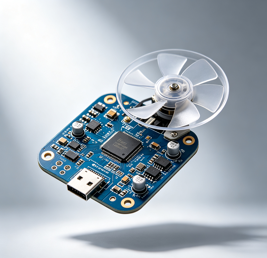
In the rapidly evolving world of industrial automation, the Industrial IoT Gateway PCB stands as a cornerstone of connectivity and efficiency. At hcdpcba, we pride ourselves on delivering cutting-edge solutions that bridge the gap between devices and data streams, ensuring seamless integration in demanding environments. This pivotal component forms the backbone of industrial Internet of Things (IoT) systems, enabling real-time monitoring, control, and data analysis across factories, warehouses, and remote operations. With our expertise in PCB design and assembly, hcdpcba crafts Industrial IoT Gateway PCBs that withstand harsh conditions while optimizing performance for smart manufacturing.
Delving deeper into its design, the Industrial IoT Gateway PCB excels in handling complex data flows from sensors to cloud platforms, incorporating robust protocols like MQTT and CoAP for secure communications. Our Wireless IoT PCB variant elevates this further by integrating Bluetooth, Wi-Fi, and cellular modules, allowing for flexible deployment in wireless networks without compromising on reliability. hcdpcba's state-of-the-art facilities ensure that every Wireless IoT PCB undergoes rigorous testing, from signal integrity checks to environmental stress simulations, guaranteeing longevity in applications such as predictive maintenance and asset tracking. This wireless capability not only reduces cabling costs but also enhances scalability, making it ideal for expanding IoT ecosystems in industries like automotive and energy.
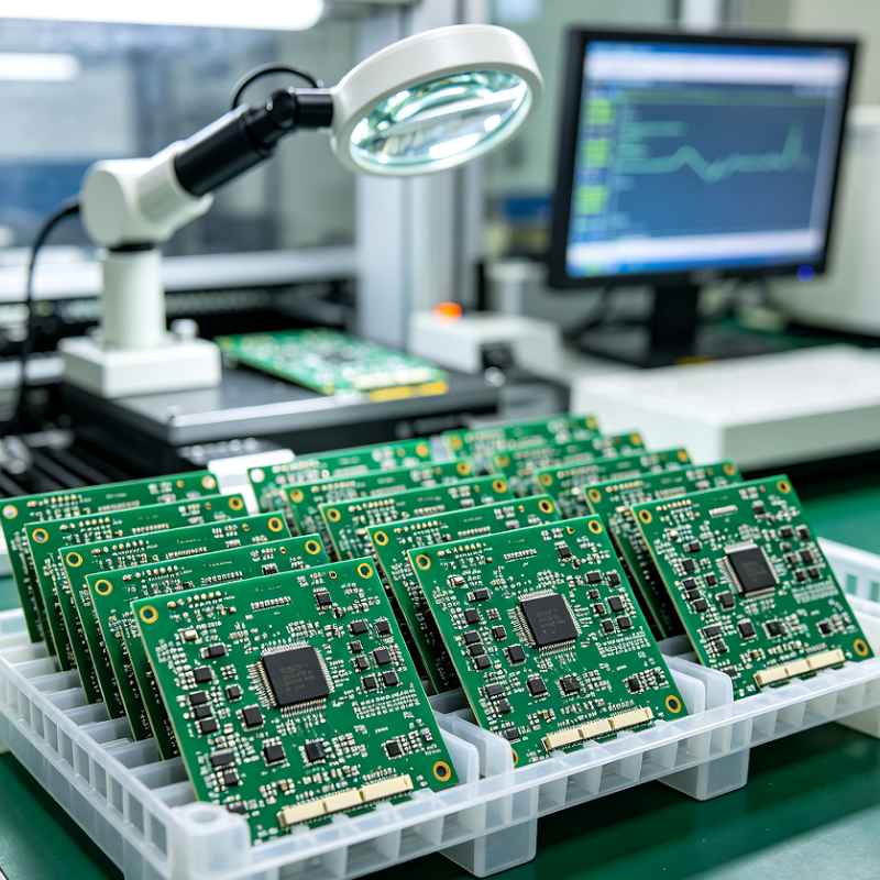
When it comes to production, hcdpcba's IoT Device PCB Assembly services transform innovative designs into functional realities with precision and speed. We specialize in high-volume SMT placement and advanced soldering techniques, ensuring that each IoT Device PCB Assembly meets the stringent standards of sectors like medical devices and smart homes. Our comprehensive process includes component sourcing from trusted suppliers, automated assembly lines, and thorough functional testing to eliminate defects early. Complementing this, our IoT Gateway PCB Design team collaborates closely with clients to incorporate features like edge computing and power optimization, resulting in compact, energy-efficient boards that drive operational excellence.
hcdpcba's commitment to quality is evident in every stage, from initial prototyping via our rapid PCB sampling service to full-scale OEM and ODM production. For Industrial IoT Gateway PCBs, we apply DFMA principles to minimize assembly complexities and costs, while our AOI systems provide optical inspections that detect even the minutest imperfections, ensuring zero-defect outputs. This meticulous approach supports diverse applications in industrial control, security, and telecommunications, where reliability is non-negotiable. Clients benefit from our fast response times, cost-effective solutions, and stringent confidentiality measures, fostering long-term partnerships.
Looking ahead, the integration of Industrial IoT Gateway PCBs with emerging technologies like AI and 5G promises to revolutionize industries. At hcdpcba, we are at the forefront, offering tailored Wireless IoT PCB solutions that adapt to future demands, alongside expert IoT Device PCB Assembly for custom needs. Whether you're developing gateways for power grids or intelligent factories, our IoT Gateway PCB Design services ensure your products are future-proof. With over a decade of experience, hcdpcba continues to empower innovation, delivering boards that not only connect but also transform operations into smarter, more efficient paradigms. Embrace the power of reliable IoT hardware with us today, and witness the difference in your project's success.
Loading...