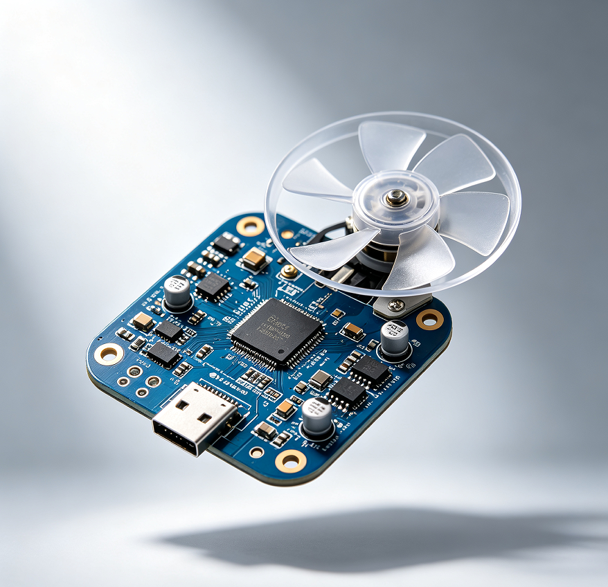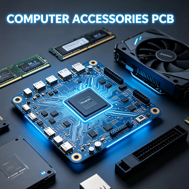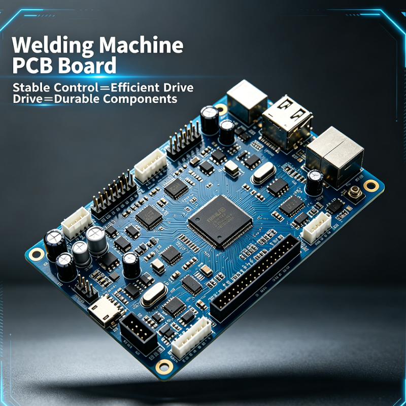
In the rapidly evolving world of energy storage and electric vehicle technology, the High-Voltage BMS PCB stands out as a pinnacle of innovation from hcdpcba. This advanced printed circuit board is meticulously engineered to manage and safeguard high-voltage battery systems with unparalleled precision and reliability. As a core component in modern power solutions, the High-Voltage BMS PCB ensures optimal performance by monitoring voltage levels, balancing cells, and preventing overcharge or discharge scenarios. At hcdpcba, our commitment to excellence shines through in every layer of this board, designed to meet the stringent demands of industries like automotive electronics and renewable energy. With our expertise in PCBA boards, including multi-layer and HDI variants, we deliver a product that not only integrates seamlessly into battery packs but also enhances overall system efficiency.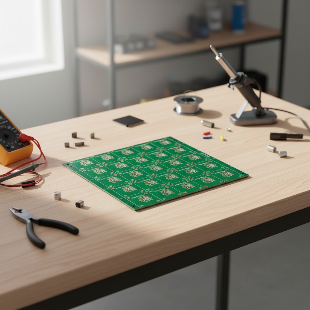
Delving deeper into its capabilities, the High-Voltage BMS PCB features a high-density QFN array layout that optimizes space while maximizing electrical performance and thermal management. This design is particularly vital for compact applications where every millimeter counts, such as in electric vehicles or portable power devices. Complementing this is our Battery Pack Control PCB functionality, which orchestrates the intricate dance of power distribution across multiple cells, ensuring longevity and safety. hcdpcba's state-of-the-art SMT pasting services bring this vision to life, employing professional equipment to handle diverse components with pinpoint accuracy. Imagine a board that withstands extreme voltages up to several hundred volts, thanks to gold-plated contacts and robust material compositions that minimize signal loss and boost conductivity. Our Battery Monitoring PCB aspect further elevates this by providing real-time data on temperature, current, and state-of-charge, empowering users with actionable insights to prevent failures before they occur. Drawing from our comprehensive services like PCB prototyping and component sourcing, this PCB is tailored for innovators who demand both customization and scalability.
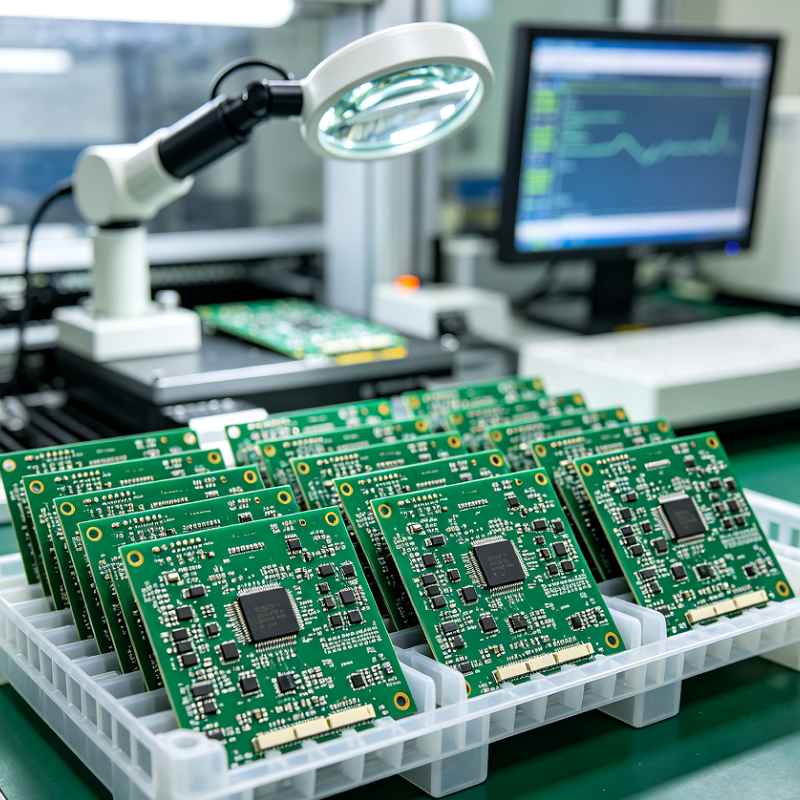
What sets hcdpcba's High-Voltage BMS PCB apart is its seamless integration into broader production ecosystems, supported by our OEM and ODM offerings. Whether you're developing smart home energy storage or industrial automation systems, this board's symmetrical layout and advanced packaging ensure durability in harsh environments. Our DFMA services analyze designs for manufacturability, reducing costs without compromising quality, while rigorous testing protocols guarantee zero-defect outcomes. Clients in fields like IoT, medical devices, and telecommunications have already harnessed the power of our Battery Pack Control PCB to achieve breakthroughs in efficiency. The High-Voltage BMS PCB isn't just a component; it's a gateway to reliable, high-performance energy management. With features like efficient thermal conductivity and support for high-speed processing, it aligns perfectly with the needs of cutting-edge applications. At hcdpcba, we pride ourselves on rapid response times, cost-effective solutions, and stringent confidentiality, making us the trusted partner for your next project.
Exploring further, the Battery Monitoring PCB embedded within our High-Voltage BMS PCB lineup offers versatile applications across diverse sectors. From securing power in AI-driven robots to stabilizing grids in smart cities, this technology embodies resilience and precision. hcdpcba's experienced team provides technical support at every stage, from initial prototyping to full-scale assembly, ensuring your vision translates into a market-ready product. The use of high-frequency materials and multi-layer constructions allows for superior signal integrity, even under demanding loads. As we continue to push boundaries in PCB technology, our High-Voltage BMS PCB remains at the forefront, inviting engineers and developers to unlock new potentials in battery management. Contact us at +86 18924624188 to discuss how this innovative solution can electrify your projects with safety and sophistication.
Loading...