Camera PCBA for Compact Imaging Modules and Embedded Vision Systems
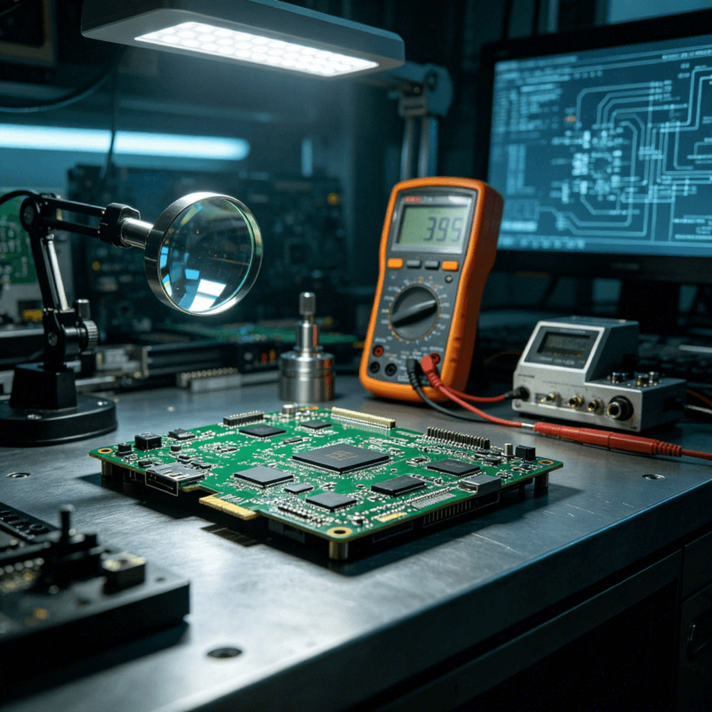
A camera pcba is the backbone of a small imaging device when the buyer needs a stable way to capture images or video without fighting layout, wiring, or alignment problems. In compact electronics, the challenge is rarely just “adding a camera”; it is fitting the sensor, lens, connectors, and support circuitry into a controlled assembly that can survive handling, testing, and integration into the final product. This type of board assembly is commonly used where space is tight and image capture must be built directly into the device architecture.
Product Overview
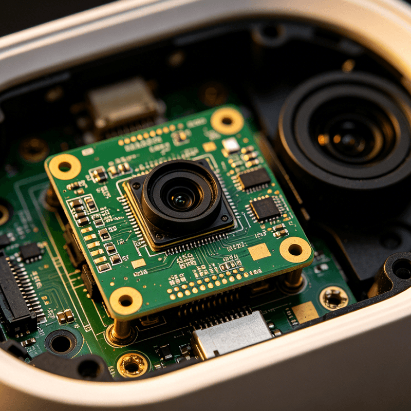
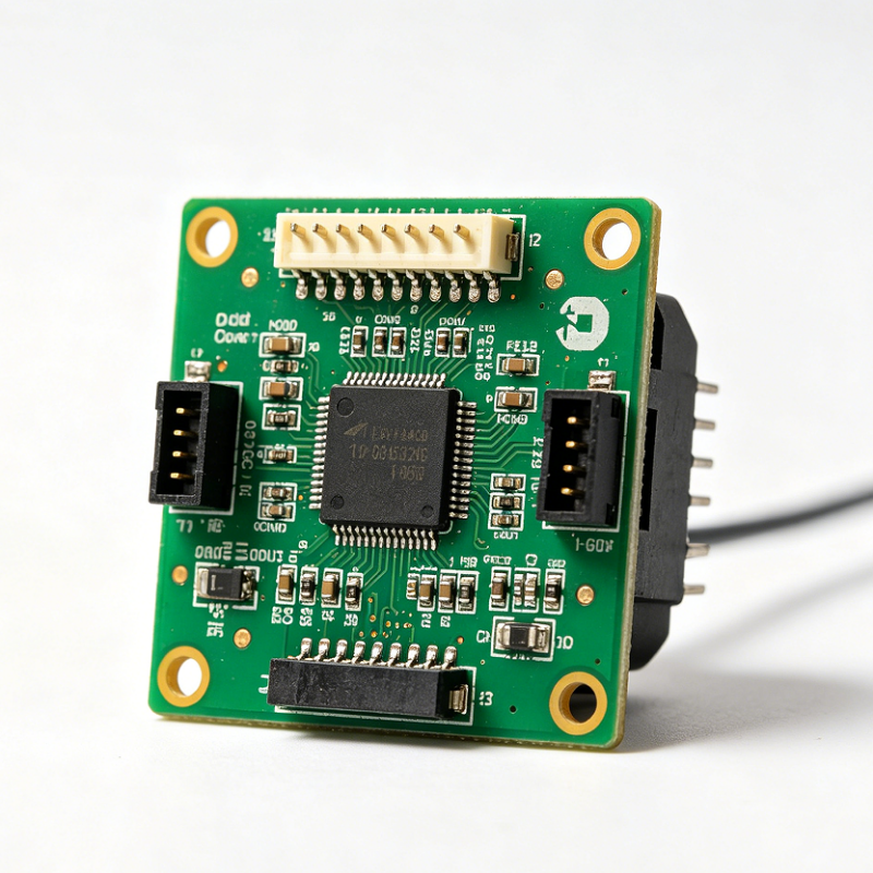
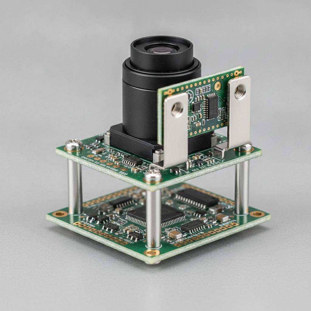
The visible product category here is an embedded camera module / camera sensor board assembly. The structure suggests a PCB-based imaging unit with a central sensor board mounted on standoffs above a larger main board. Gold-plated contact pads, mounting holes, ICs, fine-pitch components, and a lens housing indicate a complete electronic subassembly rather than a bare board. The form factor is compact, which matters in products that need optical sensing but cannot spare much internal volume.
For buyers, this kind of assembly solves a practical problem: it combines imaging electronics and mechanical support in one buildable unit. That makes integration easier for consumer devices, robots, inspection tools, drones, and security products. Depending on the design, it may also fit into a broader ipc pcba workflow where imaging boards are produced alongside other control or interface boards.
Key Specifications and Visible Capabilities
Board structure
The assembly shows a green FR-4 base board with a smaller square sensor section mounted above it. The use of standoffs and screws suggests a layered mechanical arrangement intended to hold the optical center in place. This kind of geometry is common when the sensor must be positioned carefully relative to the lens stack.
Electronic features
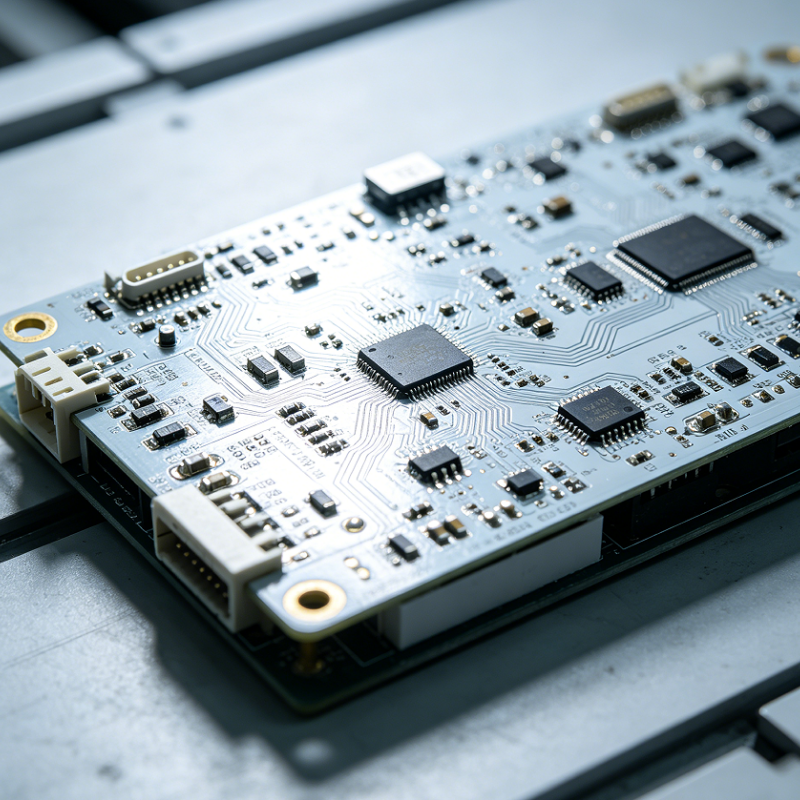
Visible components include integrated circuits, connectors, surface-mount parts, and exposed plated pads. These details indicate a populated board ready for further integration or test. The assembly looks designed for precise electrical connection as well as optical capture.
Optical module elements
A black lens housing sits near the sensor area. The image does not confirm resolution, focal length, aperture, or field of view, so those should be defined by the buyer’s project requirements rather than assumed. What can be verified is the presence of a lens stack and a sensor-centered layout suitable for embedded imaging.
Materials and Finish Options
The visible base material appears to be FR-4, a common printed circuit board substrate used in many electronics assemblies. Plated contact pads show a gold-colored finish, which is often selected for reliable mating and stable conductivity in connectors or test points. The mechanical parts appear to include black plastic or metal lens housings and a light silver outer shell or coated structure.
In real-world projects, finish choices may vary by application. Buyers typically specify solder mask color, surface finish, connector style, shielding needs, and any protective coating based on the environment the board will face. For a security camera pcba or cctv camera circuit board, enclosure compatibility and connector reliability often matter as much as the optical side.
Manufacturing and Assembly Process
This kind of module is likely produced through SMT placement, sensor mounting, lens alignment, and mechanical fastening. Because the image shows a tightly integrated optical-electronic unit, the work may also include inspection and calibration steps to verify board condition and alignment. Exact process details are not visible, so they should be treated as likely rather than certain.
For buyers ordering a surveillance camera pcb assembly or a machine-vision subassembly, the critical manufacturing point is repeatability. A sensor that shifts slightly, a connector that sits out of plane, or a lens that is not aligned cleanly can affect the final imaging result. That is why assembly discipline matters so much in camera boards compared with ordinary control PCBs.
Where This Type of PCB Assembly Is Used
Camera modules like this are suited to consumer electronics cameras, inspection devices, robotics, drones, industrial vision equipment, and security systems. In factory environments, they may sit inside inspection heads, barcode readers, monitoring units, or guided automation platforms. In security applications, the module may be integrated into a fixed camera housing or a multi-sensor platform that watches entrances, corridors, or equipment zones.
In high-mix manufacturing, the same base approach can be adapted into different product families. A buyer developing an embedded vision device may need one design for a small mobile product and another for a harsher industrial enclosure. The underlying camera pcba concept remains the same, but the board stack, connector layout, and support hardware shift with the system requirements.
Quality Control and Inspection Considerations
Camera boards are typically checked in more than one way. Visual inspection confirms component placement, solder quality, and mechanical fit. Electrical testing helps confirm that the board powers correctly and that signals route as intended. Optical inspection may be added when the module includes a lens and image sensor, because mechanical position can influence image usability.
hcdpcba also supports assembly and testing services, along with DFMA guidance, which can help reduce manufacturing risk before the design reaches production. For buyers, that matters when a board needs to move from prototype to repeatable build without rewriting the whole design.
Customization Guidance for Buyers
When specifying a camera board, the main decision points are mechanical size, connector position, lens arrangement, supported interface, power budget, and target use environment. If the board will sit in a compact enclosure, the height of the lens stack and the location of mounting holes can affect the entire device layout. If the board will be used in inspection or industrial automation, connector retention and fixture compatibility become more important.
Before placing an order, buyers should define the application clearly: is it a security camera pcba, a lab prototype, or a subassembly for a larger vision system? From there, the board stack, materials, finish, and test plan can be matched to the product’s job. For OEM and ODM projects, that clarity saves time during sample validation and mass production.
Why This Assembly Format Works Well
The layered construction, visible mounting hardware, and dense component population make this a practical choice for embedded imaging. It is compact, serviceable, and suitable for careful electrical and mechanical integration. When paired with disciplined SMT work and inspection, the format supports reliable camera module production across different industries.
Contact and Next Steps
If you are developing a camera pcba for a new device, share your board outline, lens requirements, interface needs, and expected application environment. hcdpcba can support PCB prototyping, SMT assembly, parts sourcing, assembly, testing, and custom OEM/ODM workflows. For project discussion, contact +86 18924624188 and provide the product goals, so the build can be matched to the real use case rather than guessed from a generic spec sheet.