


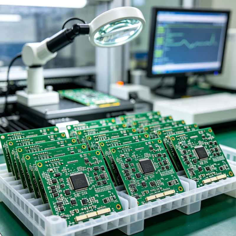
In the rapidly evolving world of connected devices, WiFi IoT PCB Assembly stands out as a cornerstone for seamless integration and high-performance electronics. At hcdpcba, we specialize in crafting these advanced assemblies that empower your IoT projects with reliable wireless connectivity. Our WiFi IoT PCB Assembly services utilize state-of-the-art multilayer technology, ensuring exceptional signal integrity and robust data transmission even in demanding environments. Imagine transforming your ideas into reality with PCBs that handle complex WiFi protocols effortlessly, supporting everything from smart home systems to industrial sensors. This precision engineering not only enhances device efficiency but also minimizes latency, making it ideal for real-time applications.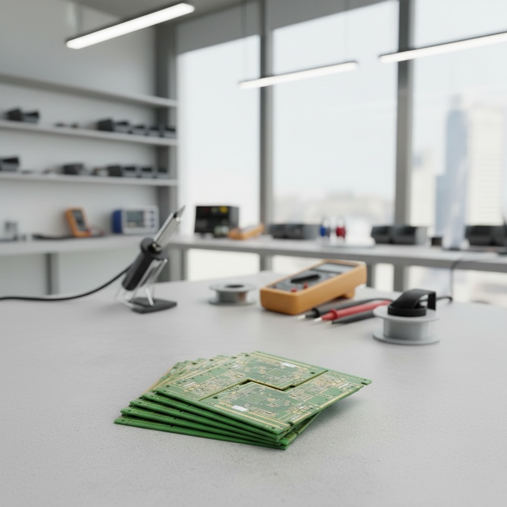
Building on our expertise, hcdpcba extends its capabilities to LoRa IoT PCB solutions, which are perfect for long-range, low-power communications in remote monitoring setups. These LoRa IoT PCB boards are designed with energy-efficient components that extend battery life while maintaining strong signal penetration through obstacles. Complementing this, our NB-IoT PCB Assembly offers narrowband connectivity tailored for massive machine-type communications, ensuring low-cost, wide-area coverage for urban and rural deployments alike. Each assembly process at hcdpcba incorporates rigorous quality controls, from SMT placement to final testing, guaranteeing durability and compliance with international standards. Whether you're prototyping a sensor network or scaling production, our IoT PCB Manufacturing process streamlines every step, reducing time-to-market without compromising on reliability.
Delving deeper into our offerings, IoT PCB Manufacturing at hcdpcba encompasses a full spectrum of services, including component sourcing, assembly, and comprehensive testing to validate functionality. For WiFi IoT PCB Assembly, we employ high-frequency materials that resist interference, ensuring your devices operate flawlessly in crowded WiFi spectra. Our LoRa IoT PCB designs incorporate optimized antenna layouts for superior range, making them indispensable for agriculture or environmental monitoring projects. Similarly, NB-IoT PCB Assembly focuses on compact footprints with integrated power management, ideal for wearable tech or asset tracking. With our DFMA services, we analyze designs early to optimize manufacturability, cutting costs and enhancing assembly yields. hcdpcba's OEM and ODM capabilities mean we can customize these solutions to fit your exact specifications, from high-density interconnects to thermal management features that prevent overheating in continuous operations.
What sets hcdpcba apart is our commitment to excellence across all facets of IoT PCB Manufacturing. Our experienced team provides rapid prototyping through PCB打样 services, allowing you to iterate designs quickly with multi-layer support up to advanced specifications. For WiFi IoT PCB Assembly, we ensure seamless integration with microcontrollers and modules, backed by our 元器件代采 for authentic, high-quality parts. LoRa IoT PCB projects benefit from our scientific assembly workflows that boost efficiency, while NB-IoT PCB Assembly includes thorough functional tests to detect and resolve issues proactively. Serving diverse industries like industrial control, medical devices, automotive electronics, and smart homes, our products drive innovation in IoT ecosystems. With strict quality assurance, fast response times, and cost-effective processes, hcdpcba delivers zero-defect solutions protected by robust confidentiality measures. Elevate your next project with our versatile, cutting-edge PCBs—contact us at +86 18924624188 to start building the future of connected technology today.

People who viewed this also viewed

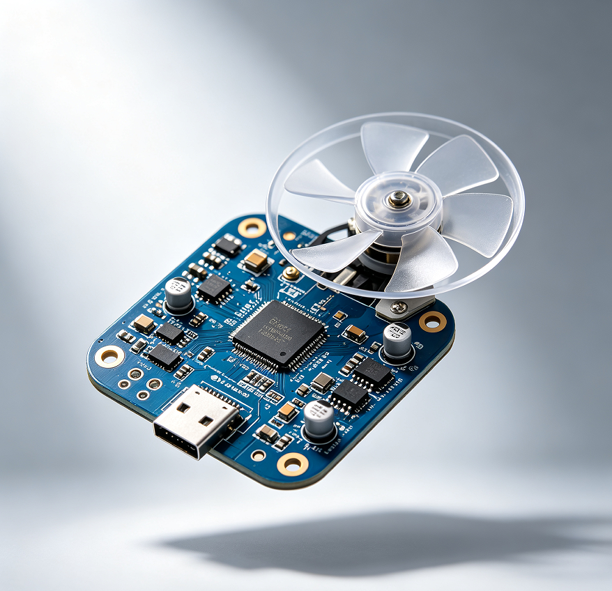
1. Hand Fan PCB A Overview 2. Product Structure and Visible Features 3. Key Specifications and Capabilities 4. Materials and Finish Options 5. Manufacturing and Assembly Process 6. Application Scenarios 7. Quality Control Considerations 8. Customization Guidance for Buyers 9. How to Evaluate Fit for Your Project 10. Request Custom PCB and Assembly Support

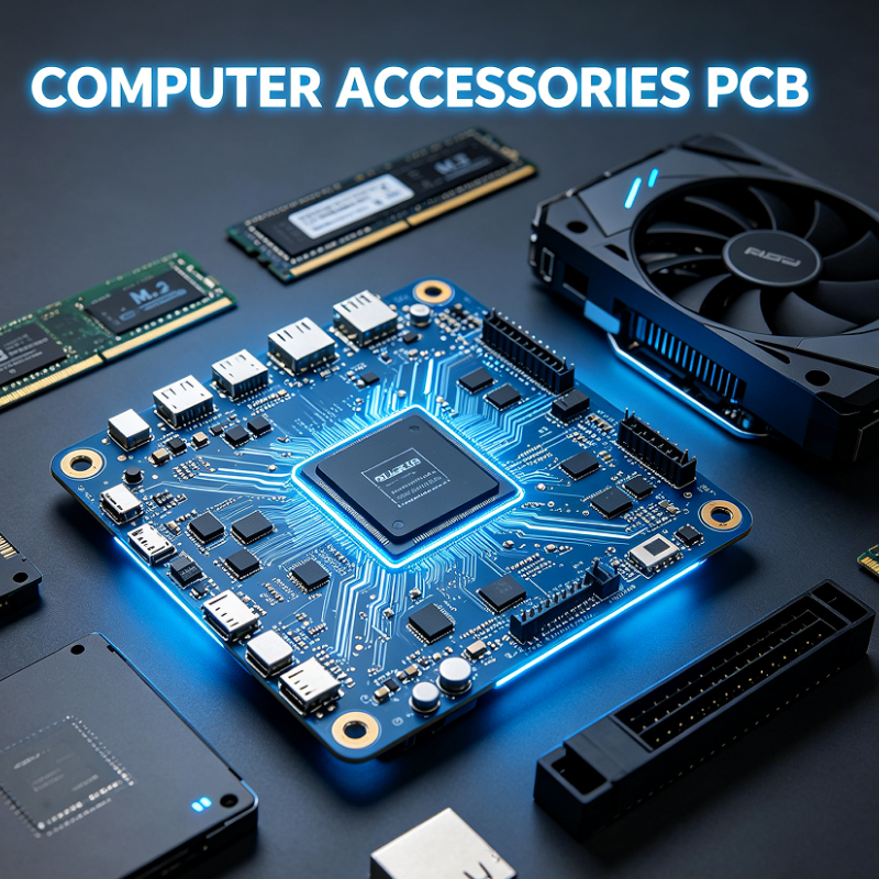
1. Computer Accessories PCB Overview 2. Product Structure and Visible Features 3. Key Capabilities and Board-Level Functions 4. Materials and Finish Options 5. Manufacturing Process and PCBA Service Flow 6. Application Scenarios 7. Quality Control and Buyer Decision Factors 8. Customization Guidance 9. Request a Custom Quote

1. Medical Grade PCB for Controlled, Reliable Electronic Modules 2. Product Overview 3. Key Features and Capabilities 4. Materials and Finish Options 5. Manufacturing Process 6. Where These Boards Are Used 7. Quality Control Considerations 8. Customization Guidance for Buyers 9. Decision Factors Before Ordering 10. Request PCB Assembly Support

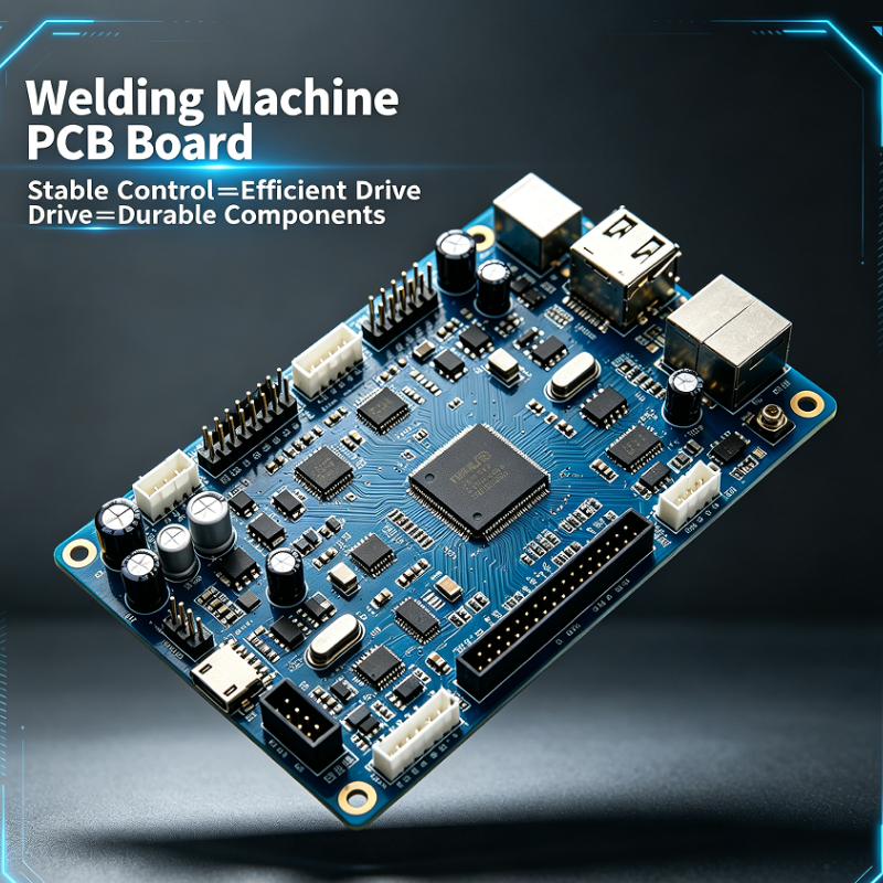
1. Welding Machine PCB Board Overview 2. Product Overview 3. Key Capabilities and Design Features 4. Materials and Finish Options 5. Manufacturing Process 6. Application Scenarios 7. Quality Control and Testing 8. Customization Guidance for Buyers 9. How to Evaluate the Right Supplier 10. Request a Custom Quote