
Power Optimizer PCBA Overview
A Power Optimizer PCBA is used to solve a common solar problem: one underperforming panel can drag down the output of a whole string. By moving power optimization to the module level, this board supports per-panel MPPT, helps improve shade tolerance, and adds rapid shutdown functions for safer photovoltaic system operation. For buyers building module-level power electronics, the value is not only energy harvest, but also easier integration of monitoring and safety control into the PV module path.
What the Board Does
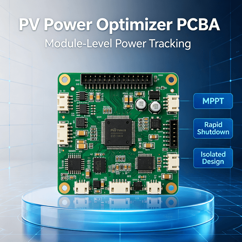
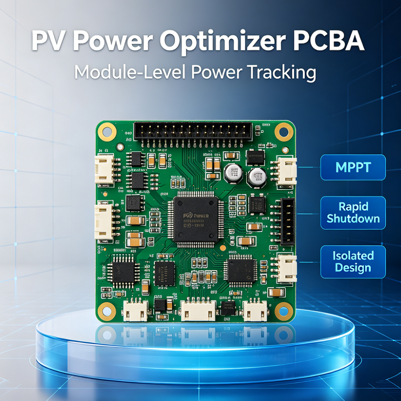
Based on the provided product data, this is a photovoltaic optimizer PCB assembly intended for solar module-level power electronics. The visible labels indicate three core functions: MPPT, rapid shutdown, and isolated design. Another set of visible claims points to single-module MPPT, shade performance improvement, fast power shutdown, and integrated monitoring. That combination makes the board relevant for residential and commercial solar systems where panel-level control is preferred over string-only behavior.
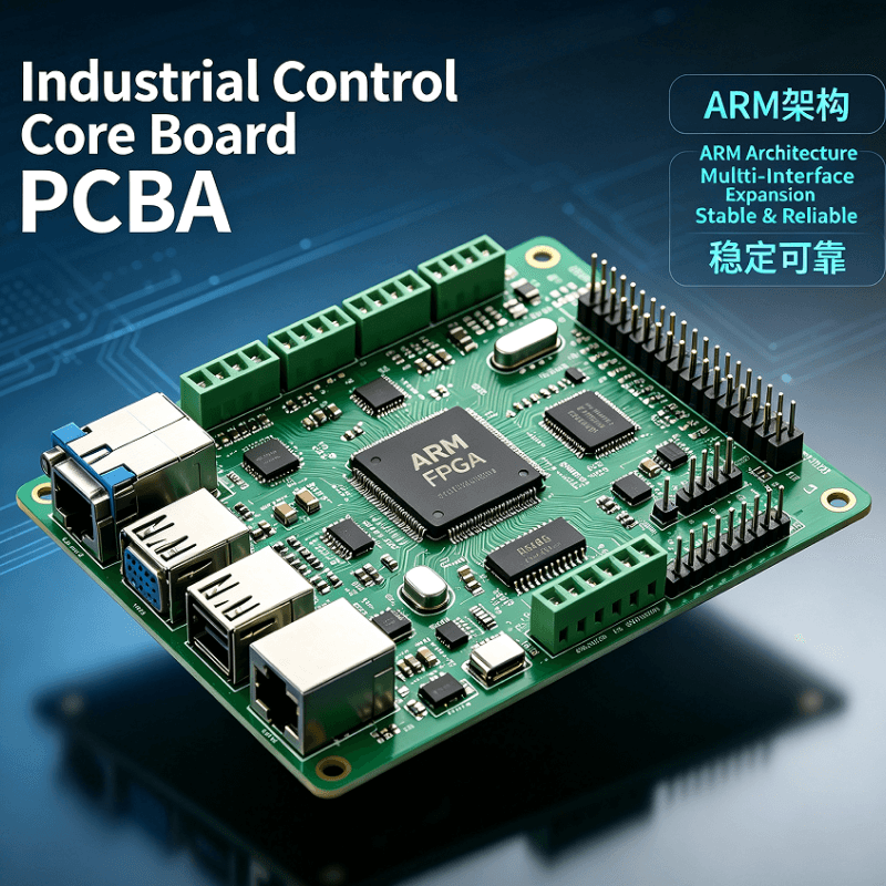
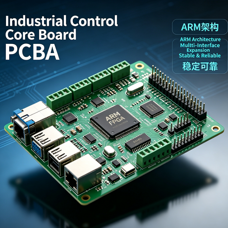
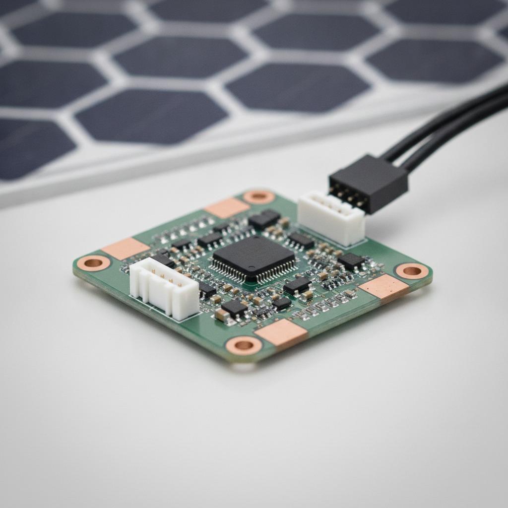
The board shown is a compact square PCB with rounded corners, four corner mounting holes, several edge connectors, and a dense mix of ICs and passive components. The central control IC and surrounding support devices suggest embedded power management or control logic, but exact circuit topology is not provided. It should be treated as a PCBA for photovoltaic use rather than a fully specified finished product unless confirmed by the buyer’s documentation.
Key Specifications and Visible Capabilities
Observable structural features
The image shows a standard electronic assembly layout with surface-mount components, board-edge connectors, and plated mounting holes. The finish appears to be a solder-masked PCB with exposed contact areas near interfaces. Exact laminate, copper thickness, plating stack, and board dimensions are not confirmed and should be validated during sourcing.
Functional points shown in the product data
Visible product claims include module-level MPPT, rapid shutdown, isolated design, shade performance improvement, high-voltage isolation, arc and fault protection, and integrated monitoring. These are important buyer decision points because they map directly to energy yield, system safety, and diagnostic visibility in PV deployments. However, electrical ratings, shutdown timing, efficiency, and communication protocol are not supplied and should not be assumed.
Materials and Finish Options
The visible board appears to use a green or blue solder mask depending on the source image description, with metallic pads and white plastic connectors. A standard FR-4 style substrate is likely, but that is not independently verified from the image. For a Power Optimizer PCBA, finish selection usually depends on the intended operating environment, solderability requirements, and connector strategy. Buyers often ask for options such as surface finish type, protective coating, connector selection, and board thickness; those details should be finalized through the manufacturing file set rather than inferred from a photo.
Manufacturing Process and Assembly Flow
This product category strongly suggests PCB assembly services that include SMT placement, reflow soldering, and connector installation. Because the board carries multiple ICs and dense passives, placement accuracy and solder joint consistency matter more than in simple power boards. A manufacturing partner such as hcdpcba can support PCB prototyping, SMT assembly, component sourcing, assembly, testing, and DFMA review for solar electronics programs.
For module-level power electronics, process control typically focuses on paste printing, component placement, reflow profile management, inspection, and electrical test. If the design uses through-hole or press-fit connectors, those steps can be added after SMT. Final test requirements depend on the customer’s control strategy and safety architecture.
Application Scenarios
A Power Optimizer PCBA is commonly used in photovoltaic module electronics where each panel needs independent optimization. Typical use cases include rooftop solar arrays, residential shutdown systems, commercial distributed PV installations, and OEM integrations inside optimizer modules or related safety devices. The visible functions also point to relevance in systems that require high-voltage isolation and fault-aware control logic.
For buyers working on inverter ecosystems, combiner-box integration, or module-level monitoring, this type of board can serve as a control core or a subassembly. Its compact geometry and multiple connectors suggest it is designed for embedded installation rather than stand-alone use.
Quality Control and Buyer Considerations
Quality control for solar PV PCBA work should focus on solder joint integrity, connector retention, routing cleanliness, assembly consistency, and electrical verification. The product data mentions IPC-A-610 Class 2 assembly, but that claim appears as image-provided information and should be confirmed before procurement. Other compliance badges such as RoHS 3, REACH, and UL 796 compatible are also shown in the source material and should be validated through the supplier’s documentation package.
When evaluating this board, buyers should confirm the exact function split: finished optimizer module, control board, or integration-ready PCBA. They should also define required voltage and current ranges, interface type, thermal constraints, coating needs, and test coverage. These items determine whether the assembly is suitable for a specific solar architecture.
Customization Guidance
Customization is usually needed for solar electronics. Buyers can request changes to connector positions, mounting hole layout, PCB dimensions, protective coating, assembly side count, test fixtures, and BOM sourcing strategy. hcdpcba offers OEM and ODM services, which is useful when the design must match a customer’s mechanical envelope or inverter communication scheme. If your program requires DFM support, early review can reduce rework and improve assembly stability.
Why Choose This Type of PCBA
The main value of a Power Optimizer PCBA is system-level control at the module level. Instead of accepting the lowest-performing panel in the string, the optimizer architecture helps isolate panel behavior and supports safety-related shutdown functions. That is especially relevant when roof layout, partial shading, or code-driven rapid shutdown requirements influence the design.
Contact and Next Step
If you are sourcing a Solar Optimizer PCBA or a related PV control board, prepare your schematic, BOM, stack-up, mechanical drawing, and test requirements before quoting. hcdpcba supports SMT, PCB prototyping, component procurement, assembly, testing, OEM, and ODM workflows. For project discussion or production planning, contact the team at +86 18924624188.