


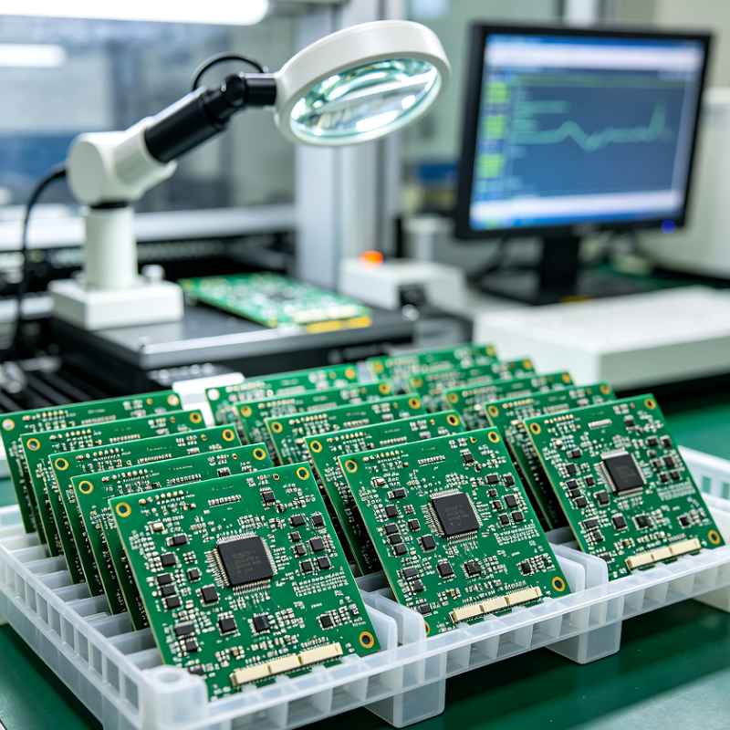
In the fast-paced world of electronics manufacturing, Consumer PCB Assembly stands out as a cornerstone for creating reliable and innovative devices. At hcdpcba, we specialize in delivering top-tier Consumer PCB Assembly services that transform your ideas into functional prototypes and production-ready products. Our expertise ensures that every board is assembled with precision, using state-of-the-art facilities to meet the demands of consumer electronics. Whether you're developing smart gadgets or everyday tech solutions, our Consumer PCB Assembly process integrates seamlessly to enhance performance and durability.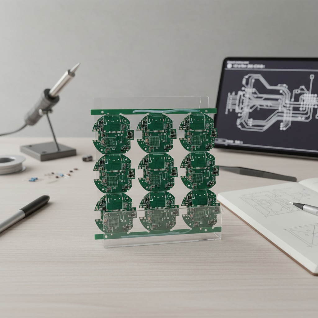
To guarantee the highest quality in Consumer PCB Assembly, we incorporate advanced inspection techniques like AOI for PCB Inspection. This automated optical method meticulously scans each board for defects, identifying issues such as misalignments or soldering errors before they impact functionality. AOI for PCB Inspection is essential in our workflow, allowing us to maintain zero-defect standards that our clients in industries like smart home devices and wearable tech rely on. Complementing this, our X-Ray Inspection PCB services provide deeper insights by revealing hidden flaws in multi-layer boards, such as voids in solder joints or internal misplacements. This non-destructive X-Ray Inspection PCB approach ensures that even the most complex assemblies are flawless, giving you confidence in every unit produced.
Beyond inspection, rigorous testing elevates our Consumer PCB Assembly to unparalleled reliability. The Aging Test PCB simulates real-world conditions by subjecting boards to extended operational stress, uncovering potential failures in components and connections. This vital step in our Aging Test PCB protocol helps predict long-term performance, making it indispensable for consumer products that must withstand daily use. At hcdpcba, our comprehensive services also include SMT placement, component sourcing, and full DFMA analysis to optimize your designs for manufacturability. Our OEM and ODM offerings mean we handle everything from prototyping via PCB sampling to large-scale production, all while adhering to strict quality controls and confidentiality agreements.
What sets hcdpcba apart in Consumer PCB Assembly is our commitment to innovation and customer-centric solutions. With a team of experienced engineers providing rapid quotes and technical support, we cater to diverse applications in IoT, automotive electronics, medical devices, and more. Our cost-effective processes, backed by efficient production lines, deliver high-value results without compromising on speed or quality. Imagine your next consumer device—sleek, efficient, and built to last—powered by our meticulously assembled PCBs that have passed AOI for PCB Inspection, X-Ray Inspection PCB, and Aging Test PCB with flying colors. Partnering with us means accessing a reliable partner who not only assembles but also accelerates your path to market success. From initial design consultations to final testing and assembly, hcdpcba is your go-to for Consumer PCB Assembly that drives technological advancement.
Our dedication to excellence is evident in every aspect of service. We procure genuine components through our efficient sourcing network, assemble with scientific precision, and test thoroughly to provide actionable feedback for improvements. This holistic approach ensures that your products meet stringent industry standards across sectors like artificial intelligence, power systems, and communications. With contact options like +86 18924624188, reaching out for a customized Consumer PCB Assembly quote is straightforward. Embrace the future of electronics with hcdpcba—where quality, efficiency, and innovation converge to bring your visions to life.

People who viewed this also viewed

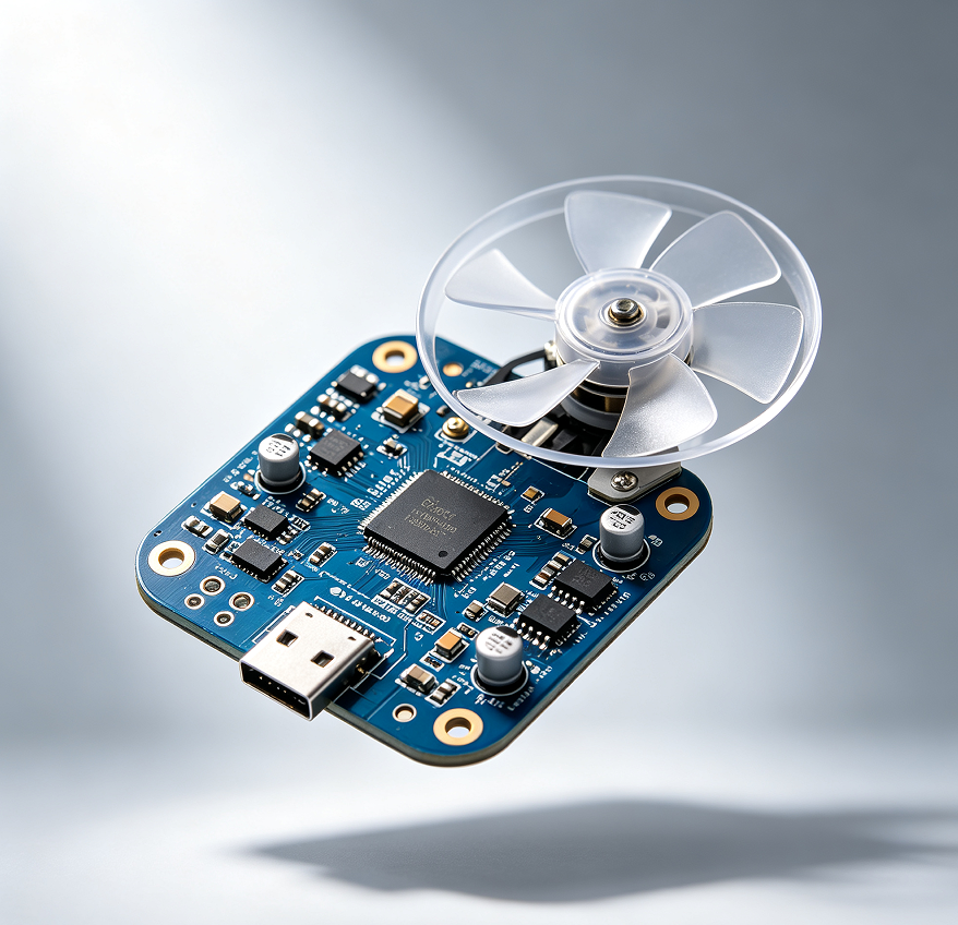
1. Hand Fan PCB A Overview 2. Product Structure and Visible Features 3. Key Specifications and Capabilities 4. Materials and Finish Options 5. Manufacturing and Assembly Process 6. Application Scenarios 7. Quality Control Considerations 8. Customization Guidance for Buyers 9. How to Evaluate Fit for Your Project 10. Request Custom PCB and Assembly Support

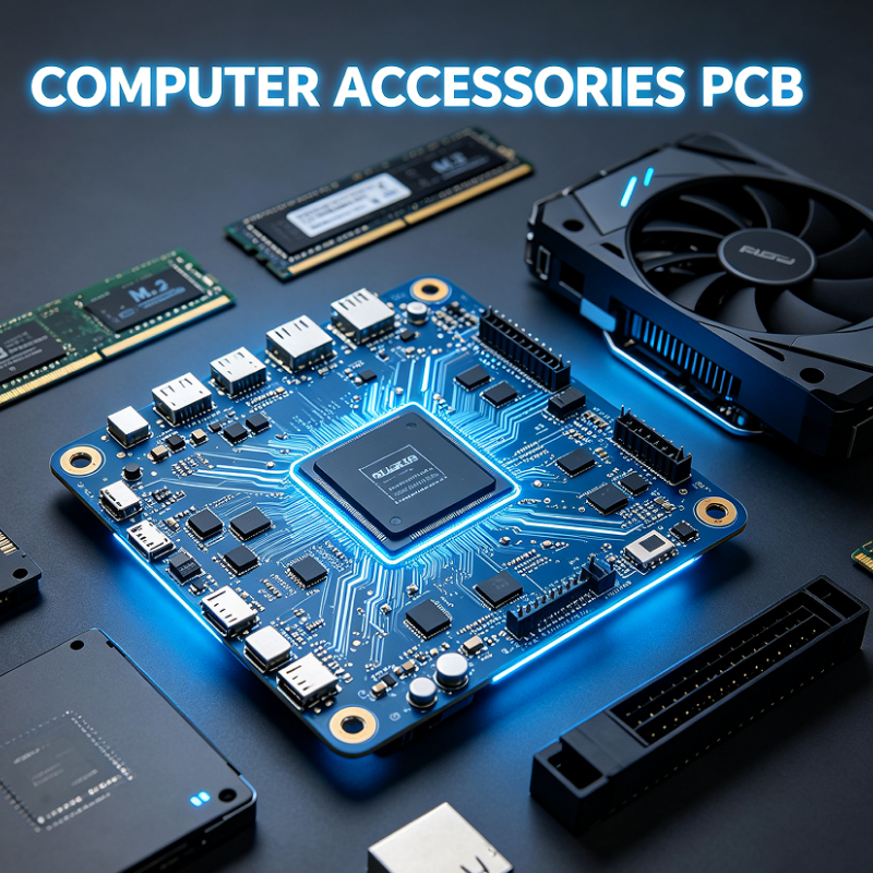
1. Computer Accessories PCB Overview 2. Product Structure and Visible Features 3. Key Capabilities and Board-Level Functions 4. Materials and Finish Options 5. Manufacturing Process and PCBA Service Flow 6. Application Scenarios 7. Quality Control and Buyer Decision Factors 8. Customization Guidance 9. Request a Custom Quote

1. Medical Grade PCB for Controlled, Reliable Electronic Modules 2. Product Overview 3. Key Features and Capabilities 4. Materials and Finish Options 5. Manufacturing Process 6. Where These Boards Are Used 7. Quality Control Considerations 8. Customization Guidance for Buyers 9. Decision Factors Before Ordering 10. Request PCB Assembly Support

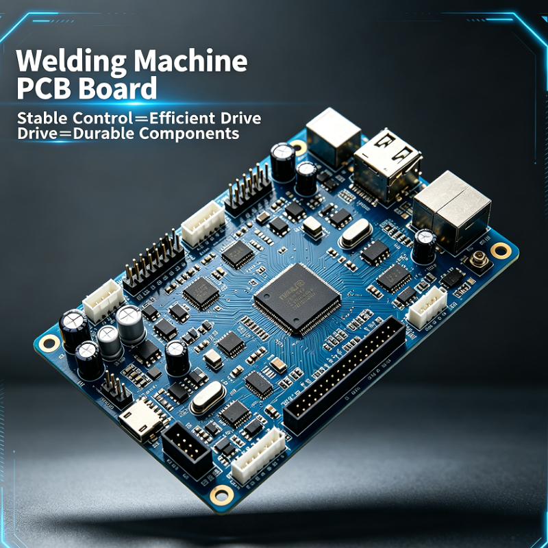
1. Welding Machine PCB Board Overview 2. Product Overview 3. Key Capabilities and Design Features 4. Materials and Finish Options 5. Manufacturing Process 6. Application Scenarios 7. Quality Control and Testing 8. Customization Guidance for Buyers 9. How to Evaluate the Right Supplier 10. Request a Custom Quote