Unlocking the Future with Wireless Communication PCB
In the rapidly evolving world of connectivity, the Wireless Communication PCB stands as a pivotal innovation, seamlessly bridging devices and networks with unparalleled efficiency. At hcdpcba, we specialize in crafting these sophisticated boards that form the backbone of modern wireless systems, ensuring reliable data transmission in everything from smart homes to industrial automation. This article delves into the intricacies of Wireless Communication PCB design, highlighting how our expertise in PCB design for wireless communication transforms ideas into robust realities.
The Essence of Wireless Communication PCB Design
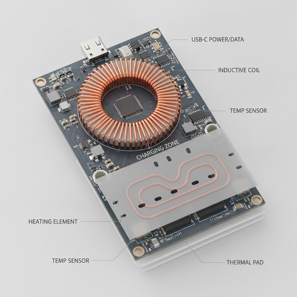
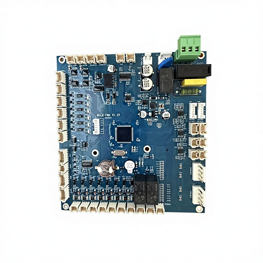
Imagine a compact, high-performance board pulsing with electromagnetic waves, facilitating instantaneous communication across vast distances. Our Wireless Communication PCB is engineered with precision, incorporating advanced materials that minimize signal loss and maximize bandwidth. At hcdpcba, we leverage years of experience in PCB design for wireless communication to create boards that support protocols like Wi-Fi, Bluetooth, and 5G, all while adhering to stringent standards for durability and heat dissipation. The sleek blue finish of our versatile control board not only enhances its aesthetic appeal but also underscores its professional-grade construction, featuring high-quality components shielded by capacitors and voltage regulators to combat noise and ensure stable operation. This design philosophy allows seamless integration of antennas and transceivers, painting a vivid picture of connectivity that powers everything from wearable tech to remote sensors.
Integrating Network Processing Board PCB for Enhanced Performance
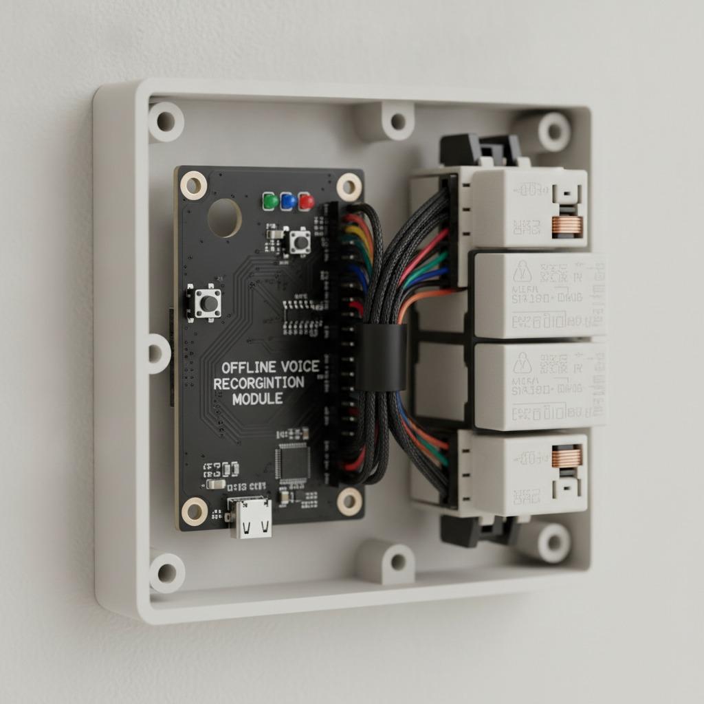
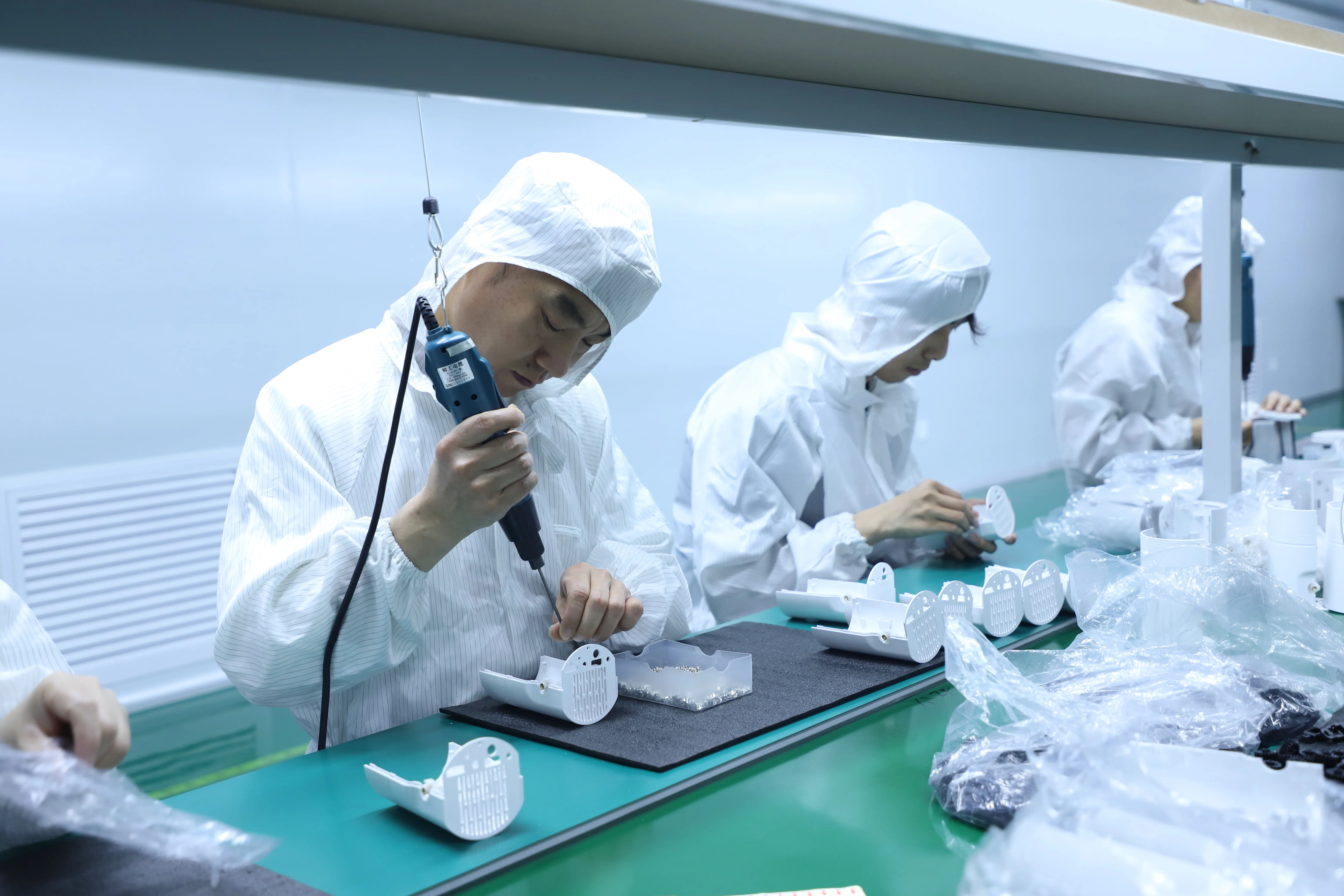
Delving deeper, the Network Processing Board PCB emerges as a critical companion to our Wireless Communication PCB, handling the intensive data flows that define today's networks. Picture a bustling digital highway where packets of information race through optimized pathways; our boards at hcdpcba make this possible with dual relays for high-power switching and myriad header pins for effortless peripheral connections. Specializing in multi-layer and HDI boards, we tailor Network Processing Board PCB solutions for applications in IoT, automotive electronics, and medical devices, ensuring low latency and high throughput. Our SMT patch services breathe life into these designs, placing components with micron-level accuracy, while our comprehensive testing verifies every signal's integrity. This holistic approach not only boosts system reliability but also vividly illustrates how hcdpcba's OEM and ODM services turn complex network demands into streamlined, innovative products that drive industries forward.
Advanced PCB Design for Wireless Communication: Innovation Meets Reliability
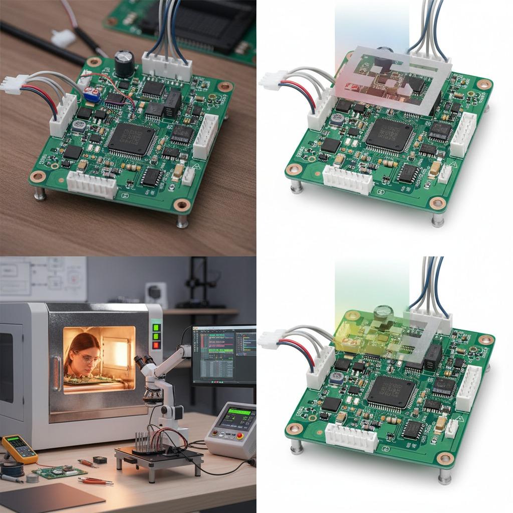
Envision a world where wireless signals dance flawlessly through crowded spectrums, unhindered by interference or failure. That's the promise of our PCB design for wireless communication at hcdpcba, where we employ DFMA services to optimize manufacturability and reduce costs without compromising quality. Our boards, including the advanced control board with on-board battery and real-time clock, safeguard data in time-sensitive scenarios like smart grids and AI-driven security systems. From rapid PCB prototyping to full-scale assembly, our response speed and technical prowess ensure that each Wireless Communication PCB and Network Processing Board PCB is a masterpiece of engineering. We procure genuine components, assemble with scientific precision, and test rigorously, all while protecting your intellectual property through strict confidentiality measures. Serving diverse sectors like telecommunications and intelligent homes, hcdpcba's cost-effective, zero-defect solutions empower your projects with the reliability and vibrancy needed to thrive in a connected era.
Why Choose hcdpcba for Your Wireless Needs
At hcdpcba, we're more than manufacturers; we're partners in innovation. Our Wireless Communication PCB offerings, complemented by expert PCB design for wireless communication, cater to a spectrum of applications with unmatched versatility. Contact us at +86 18924624188 to explore how our Network Processing Board PCB can elevate your next project, delivering the precision, performance, and peace of mind that define true technological advancement.