Unlocking Superior Performance with RF Signal Amplification PCB
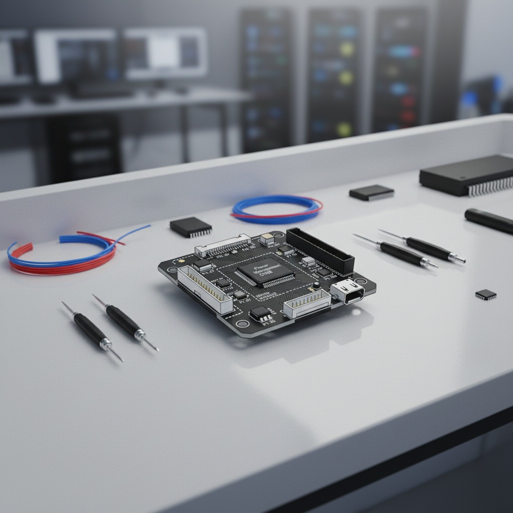
In the fast-paced world of modern electronics, the RF signal amplification PCB stands as a cornerstone for enhancing signal strength and reliability in various applications. At hcdpcba, we specialize in crafting these high-performance printed circuit boards that amplify radio frequency signals with precision and efficiency. Whether you're developing communication devices or integrating advanced sensor systems, our RF signal amplification PCB ensures that weak signals are boosted to deliver crystal-clear transmission, minimizing losses and maximizing output. This technology is vital for industries like telecommunications and IoT, where every decibel counts toward seamless connectivity.
Integrating RF Signal Amplification PCB in Communication Device PCB Designs
When designing a communication device PCB, incorporating an RF signal amplification PCB elevates the entire system's capabilities. Imagine a sleek, multi-layered board where RF components hum with optimized energy flow, amplifying signals to traverse vast distances without degradation. At hcdpcba, our expertise in PCBA boards, including high-frequency variants, allows us to customize these solutions for demanding environments such as automotive electronics or industrial controls. The RF signal amplification PCB not only boosts signal power but also integrates seamlessly with components like the CVBB Power Management chip, ensuring energy-efficient operation. Our communication device PCB services cover everything from SMT placement to full assembly, providing robust amplification that supports data rates up to gigahertz frequencies. This synergy results in devices that perform reliably, even in noisy RF spectrums, making them ideal for 5G networks or wireless sensor arrays.
Advanced Features of Our RF Signal Amplification PCB Solutions
Delving deeper, our RF signal amplification PCB features precision-engineered traces and impedance-matched layouts that prevent signal distortion, painting a picture of flawless RF pathways etched onto durable substrates. For instance, in projects involving sensor interface boards, the amplification stage enhances weak incoming signals from IoT sensors, transforming them into strong, actionable data streams. hcdpcba's commitment to quality shines through in our multi-layer HDI boards, where RF signal amplification PCB elements are paired with versatile connectors like micro-USB ports for effortless integration. We handle everything from PCB prototyping to comprehensive testing, ensuring that each board withstands environmental stresses while maintaining low noise figures. Clients in medical and security sectors rave about how our communication device PCB designs, fortified with RF amplification, deliver uninterrupted performance, reducing downtime and boosting operational efficiency.
Why Choose hcdpcba for Your RF Signal Amplification Needs
At hcdpcba, we go beyond mere manufacturing; we partner with you to bring innovative visions to life through superior RF signal amplification PCB technology. Our OEM and ODM services, backed by a team of seasoned engineers, offer DFMA analysis to streamline designs and cut costs without compromising on the vivid reliability that defines our products. Picture your next communication device PCB coming alive with amplified signals that power smart homes or AI-driven robotics— all realized through our rapid prototyping and zero-defect quality controls. With applications spanning communications, power management, and beyond, our boards are tailored to your specifications, complete with component sourcing and rigorous testing. Contact us today at +86 18924624188 to discuss how our RF signal amplification PCB can amplify your project's potential, delivering not just components, but a gateway to cutting-edge electronic excellence.
Real-World Applications and Future Innovations
The versatility of the RF signal amplification PCB extends into diverse realms, from enhancing drone communications in aerial surveillance to fortifying signals in wearable health monitors. In our Sensor Interface Board lineup, this amplification prowess integrates with ports like P1.66 and P1.97, creating a symphony of connectivity that hobbyists and professionals alike can harness. As 6G horizons emerge, hcdpcba is at the forefront, innovating communication device PCB solutions that anticipate tomorrow's bandwidth demands. Our cost-effective, confidential services ensure your intellectual property remains secure while we amplify your competitive edge. Embrace the power of amplified RF signals with hcdpcba, where every board tells a story of precision, performance, and unparalleled innovation.