Unlocking the Power of Signal Transmission PCB in Modern Electronics
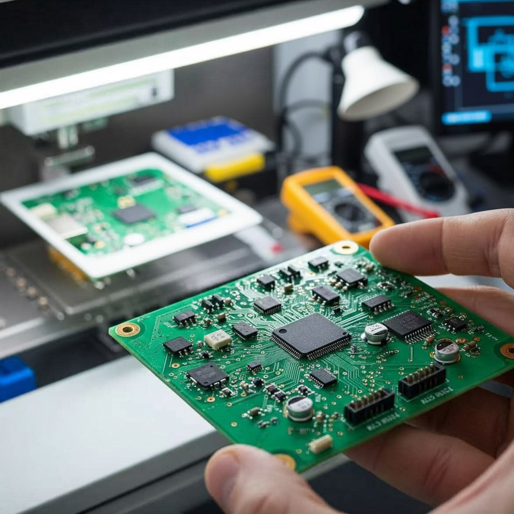
In the fast-paced world of electronics, the signal transmission PCB stands as a cornerstone for reliable data flow and connectivity. At hcdpcba, we specialize in crafting these essential components that ensure seamless communication between devices. Our cutting-edge signal transmission PCBs are designed with precision to handle intricate signals without distortion, making them indispensable for today's tech-driven applications. Whether you're developing IoT solutions or telecom infrastructure, a well-engineered signal transmission PCB guarantees optimal performance and longevity.
Integrating High Speed PCB for Demanding Environments
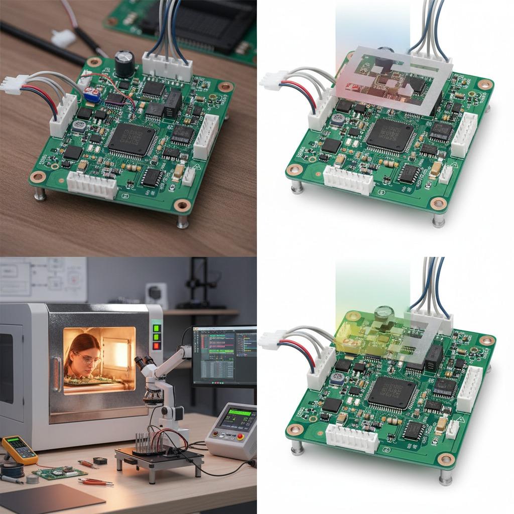
High speed PCB technology takes signal transmission to the next level, enabling rapid data transfer in environments where every millisecond counts. Imagine a compact board buzzing with energy, its multilayer structure meticulously layered to support frequencies that power everything from 5G networks to high-performance computing. At hcdpcba, our high speed PCBs feature advanced materials that minimize signal loss and electromagnetic interference, ensuring your designs run smoothly even under heavy loads. We draw on our expertise in SMT贴片 and PCBA板 production to deliver boards that not only meet but exceed industry standards, perfect for applications in automotive electronics and artificial intelligence.
Mastering RF PCB Design for Wireless Innovation
RF PCB design brings the magic of wireless communication to life, transforming invisible radio waves into tangible connections. Picture a board etched with intricate traces that dance with high-frequency signals, supporting antennas and modules that enable Bluetooth, Wi-Fi, and beyond. Our signal transmission PCBs at hcdpcba incorporate RF PCB design principles, using gold-plated contacts and durable substrates to resist oxidation and maintain signal integrity in harsh conditions. This approach is vital for telecom PCB design, where precision in layout prevents crosstalk and boosts efficiency. With our PCB打样 services, we offer rapid prototyping to help engineers iterate designs quickly, ensuring your RF projects launch with confidence.
Telecom PCB Design: The Backbone of Connectivity
Telecom PCB design is where reliability meets scalability, forming the neural network of global communication systems. Envision a robust board facilitating voice, data, and video streams across vast distances, its high-density interconnects (HDI) weaving a web of uninterrupted transmission. hcdpcba's telecom PCB designs integrate seamlessly with our signal transmission PCB offerings, supporting multi-layer configurations ideal for networking equipment and base stations. Our comprehensive services, including 元器件代采, 组装, and 测试, ensure every board undergoes rigorous quality checks for zero defects. This end-to-end support, combined with DFMA服务, optimizes manufacturability and reduces costs, empowering clients in communications and IoT sectors.
Why Choose hcdpcba for Your PCB Needs
At hcdpcba, we're more than a manufacturer; we're your partner in innovation. Our experienced team provides OEM and ODM services tailored to industries like medical devices, smart homes, and power systems. With a commitment to fast response times—quoting and producing within tight deadlines—we safeguard your project timelines. Our cost advantages stem from optimized production flows, while strict confidentiality measures protect your intellectual property. Dive into the world of high-performance electronics with our signal transmission PCBs, high speed PCB solutions, RF PCB design, and telecom PCB design expertise. Contact us at +86 18924624188 to elevate your next project with precision and reliability that sets you apart.