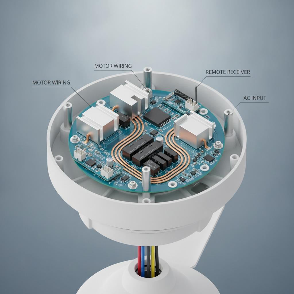
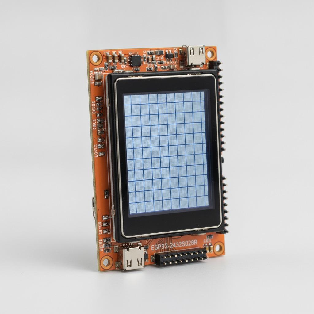
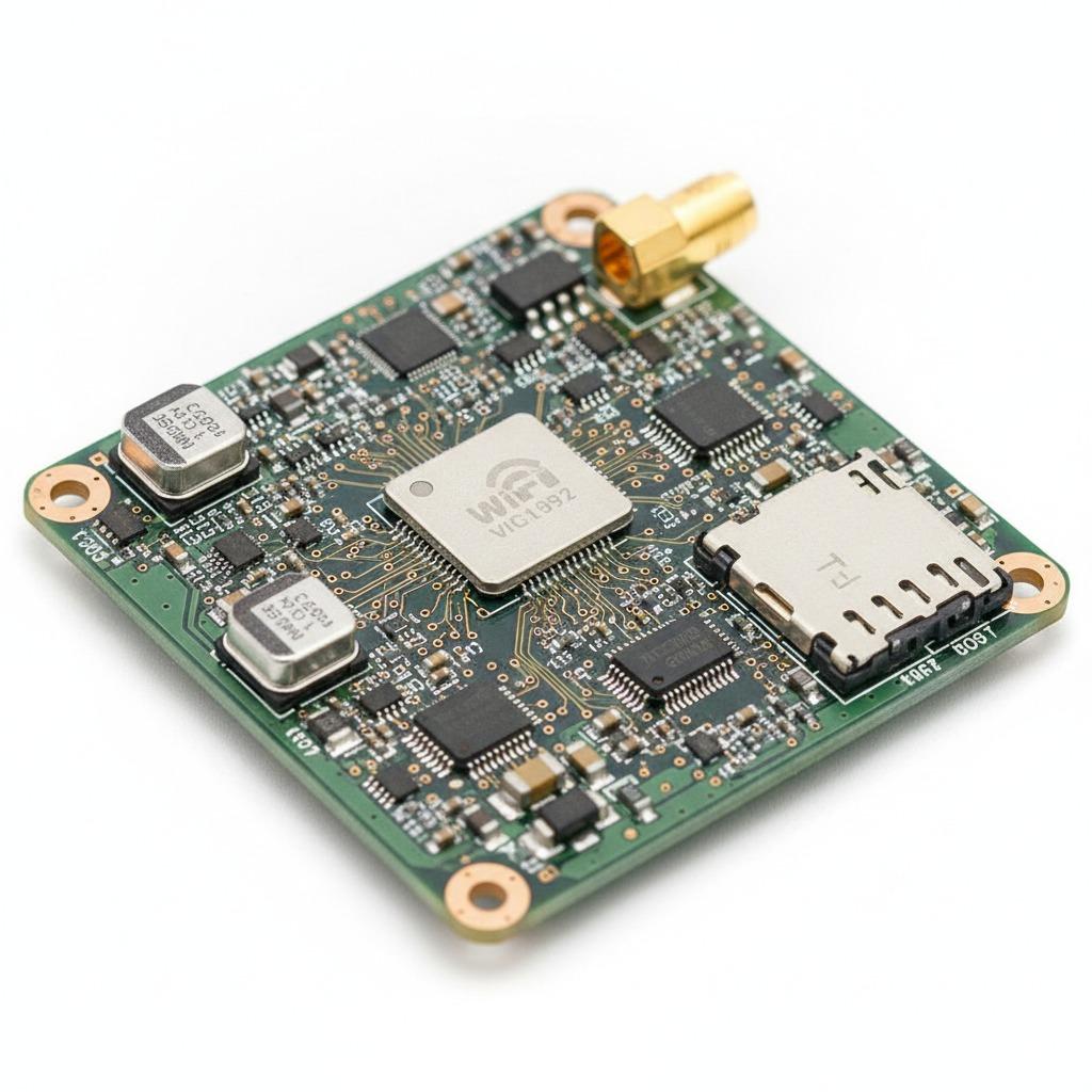
In the silent, humming world of modern technology, a complex dance of precision and engineering gives life to the devices we depend on daily. At the very heart of this electronic ecosystem lies the process of PCBA board manufacturing, the intricate art and science of creating the functional brain for everything from smartphones to spacecraft. A Printed Circuit Board Assembly (PCBA) is far more than just a green board with metallic lines; it is a meticulously crafted nerve center, a miniature city where thousands of components communicate in perfect harmony to execute commands and process information, making our digital lives possible.
The Bare Board: Understanding the PCB
A PCBA begins its life as a simple Printed Circuit Board (PCB). Picture this as the undeveloped landscape upon which a bustling metropolis will be built. The board itself is typically made from a rigid, non-conductive substrate material like FR-4 fiberglass, which provides the structural foundation. Laminated onto this substrate are one or more thin layers of copper foil. Through a process of photolithography and chemical etching, unwanted copper is removed, leaving behind a predetermined pattern of conductive pathways, or traces. These shimmering copper lines are the streets and highways of our future electronic city, designed to guide electrical signals precisely where they need to go. Holes, known as vias, are drilled to connect different layers, creating a multi-dimensional network of circuits on a single, compact board.
Populating the Board: The Art of Assembly
With the blueprint laid out on the bare PCB, the assembly process begins. The first step is the application of solder paste. A stainless steel stencil, which is a thin sheet of metal with laser-cut openings, is placed perfectly over the board. A squeegee-like blade then moves across the stencil, depositing a precise amount of solder paste onto the component pads. The consistency and location of this paste are critical, acting as both a temporary adhesive and the eventual permanent electrical connection. Following this, the board moves to a pick-and-place machine. This marvel of automation uses high-speed robotic arms, equipped with vacuum nozzles, to pick up microscopic components from reels and trays and place them onto their designated pads on the board with incredible speed and accuracy, often placing tens of thousands of components per hour.
Forging the Connections: Reflow Soldering and Inspection
Once all the surface-mount components are nestled in the solder paste, the board embarks on a journey through a long, tunnel-like reflow oven. The board travels on a conveyor belt through several zones, each with a carefully controlled temperature profile. The temperature gradually rises to activate the flux within the solder paste and then spikes to a point where the solder melts, flowing around the component leads to form strong, permanent metallurgical bonds. As the board exits the oven, it cools in a controlled manner, solidifying the solder joints. Quality control is paramount in PCBA board manufacturing. After reflow, boards are often inspected by an Automated Optical Inspection (AOI) system. This machine uses high-resolution cameras to scan the board and compare it to a perfect reference image, flagging any potential defects like missing components, incorrect polarity, or flawed solder joints.
Ensuring Functionality: Final Steps and Testing
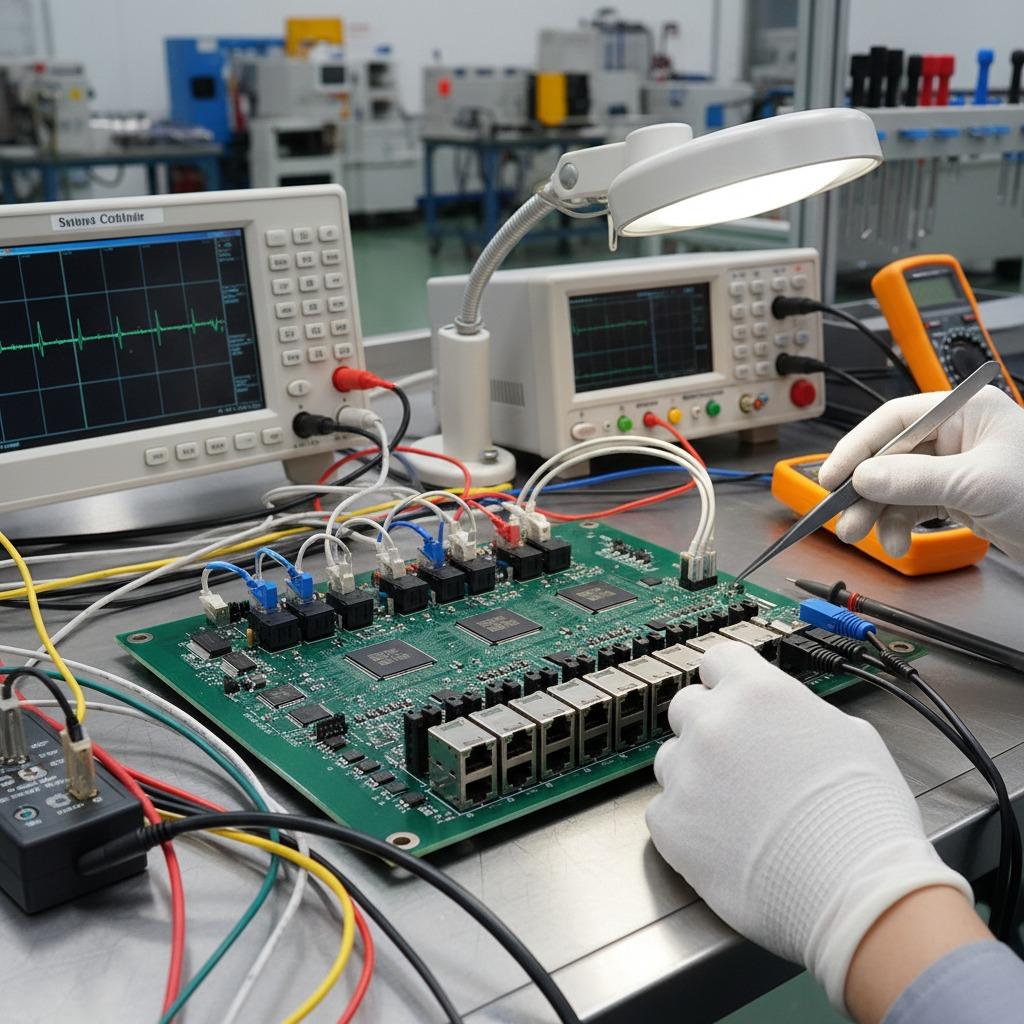
For boards that include larger, more robust components with wire leads, a process called through-hole soldering is required. These components are inserted through holes in the board, either by hand or by specialized machines, and then soldered in place. After all soldering is complete, the boards undergo a thorough cleaning process to remove any residual flux, which could cause corrosion or electrical shorts over time. The final, and perhaps most critical, stage is testing. A functional test (FCT) is performed where the completed PCBA is powered up and connected to a test fixture that simulates its intended operating environment. This test verifies that the board not only has been assembled correctly but that it performs its specific functions as designed, ensuring a reliable and fully operational electronic heart is ready to be placed into its final product.