


In the rapidly evolving landscape of modern electronics, the Communication Module PCB stands as a cornerstone of reliable connectivity and data transmission. At hcdpcba, we specialize in crafting high-performance Communication Module PCBs that integrate seamlessly into diverse applications, from industrial controls to smart home devices. These boards are engineered with precision to handle complex signal processing, ensuring minimal latency and maximum efficiency. Our commitment to quality begins with advanced manufacturing techniques, including multi-layer designs and high-frequency materials, which form the backbone of every Communication Module PCB we produce.
Delving deeper into our offerings, the 5G Communication PCB represents the pinnacle of next-generation connectivity solutions. This specialized variant of our Communication Module PCB is optimized for the demanding requirements of 5G networks, supporting ultra-high data rates and low-latency communications essential for IoT ecosystems and autonomous systems. hcdpcba's 5G Communication PCBs feature robust impedance control and shielding to mitigate electromagnetic interference, making them ideal for telecommunications, automotive electronics, and medical devices. With our SMT patch services, we ensure precise component placement, including capacitors, resistors, and microcontrollers, on vibrant green PCBs that not only perform exceptionally but also facilitate easy integration and scalability.
What sets hcdpcba apart in the realm of Communication Module PCB production is our comprehensive service ecosystem, designed to support clients from prototype to mass production. Our PCB prototyping service allows for rapid turnaround on custom 5G Communication PCB designs, often within days, enabling innovators to test and refine their concepts without delays. We handle everything from component procurement—sourcing genuine parts through our efficient agent acquisition service—to full assembly and rigorous testing protocols that verify signal integrity and thermal performance. For instance, our DFMA analysis optimizes designs for manufacturability, reducing costs by up to 20% while enhancing reliability in high-stakes environments like power systems and AI-driven applications.
Furthermore, hcdpcba's OEM and ODM capabilities extend the versatility of our Communication Module PCBs into tailored solutions for emerging technologies. Whether you're developing a 5G-enabled security system or an industrial automation hub, our experienced team provides one-on-one technical support, backed by strict quality controls that guarantee zero-defect products. Our cost advantages stem from optimized production flows and a responsive quoting system, often delivering competitive pricing without compromising on the stringent standards required for communication hardware. Clients in fields like artificial intelligence, smart energy, and consumer electronics have leveraged our 5G Communication PCBs to achieve breakthroughs, thanks to features like QR code integration for asset tracking and barcode support for streamlined inventory management.
As industries converge towards interconnected futures, hcdpcba remains at the forefront with Communication Module PCBs that embody innovation and reliability. Our application in sectors such as security, healthcare, and telecommunications underscores a proven track record, with thousands of successful deployments worldwide. By choosing hcdpcba, you're not just acquiring a board; you're partnering with a team dedicated to your success through confidential, high-speed services that protect your intellectual property and accelerate time-to-market. Contact us today at +86 18924624188 to explore how our Communication Module PCB and 5G Communication PCB can power your next project.

People who viewed this also viewed

1. Camera PCBA for Compact Imaging Modules and Embedded Vision Systems 2. Product Overview 3. Key Specifications and Visible Capabilities 4. Materials and Finish Options 5. Manufacturing and Assembly Process 6. Where This Type of PCB Assembly Is Used 7. Quality Control and Inspection Considerations 8. Customization Guidance for Buyers 9. Why This Assembly Format Works Well 10. Contact and Next Steps

1. Industrial Transmitter PCBA for Compact Industrial Measurement and Interface Modules 2. Product Overview 3. Key Specifications and Visible Capabilities 4. Materials and Finish Options 5. Manufacturing and Assembly Process 6. Application Scenarios 7. Quality Control and Integration Considerations 8. Customization Guidance for Buyers 9. Why Buyers Choose This Type of PCBA 10. Request Custom PCB Assembly Support

1. Industrial Lighting Control PCBA for Reliable Embedded Control 2. Product Overview 3. Key Capabilities and Design Features 4. Materials and Finish Options 5. Manufacturing Process 6. Typical Application Scenarios 7. Quality Control Considerations 8. Customization Guidance for Buyers 9. Why Buyers Choose a Board-Level Solution 10. Contact for Custom PCBA Projects

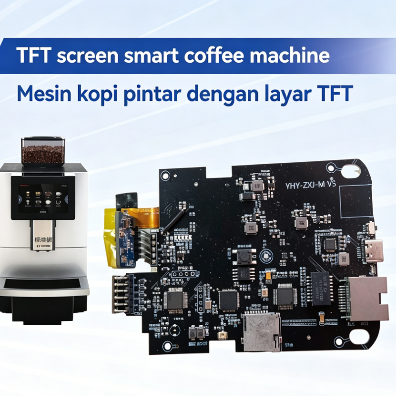
1. coffee machine pcba for smart beverage equipment 2. Product overview 3. Key visible features and capabilities 4. Materials and finish options 5. Manufacturing and assembly process 6. Typical application scenarios 7. Quality control and buyer concerns 8. Customization guidance 9. Choosing the right board for your project 10. Request OEM or ODM support