
ESP32S3 Development Board PCBA Overview
The 1. ESP32S3 development board PCBA is designed for teams that need a practical platform for firmware bring-up, wireless prototyping, and small-batch embedded validation. For buyers, the main problem it solves is speed: instead of building a custom board from scratch, you can work with a ready-made or custom-assembled PCB that already integrates the microcontroller, interface circuitry, headers, and board-level connections needed for testing IoT functions. Based on the provided product data, this board is positioned as an OEM 4-layer FR-4 HDI PCBA with immersion gold surface treatment, making it suitable for development and contract manufacturing workflows where signal routing quality and assembly consistency matter.
What the Board Is Used For
An ESP32S3-based development board is commonly used for prototyping connected devices, testing peripheral interfaces, and verifying software on Wi‑Fi/Bluetooth-enabled embedded hardware. It is also useful in early product stages when engineers need to evaluate power distribution, USB connectivity, sensor interfaces, and board-to-board connections before moving into a final design. The assembled format reduces manual wiring and shortens the path from concept to functional prototype.
Typical buyer needs
Engineers often look for a board that supports fast bring-up, stable connections, and repeated debugging without rework. Procurement teams may need a PCB circuit board assembly factory that can build small runs consistently. Product teams may need an HDI PCB assembly service that can handle dense layouts, fine-pitch SMT placement, and assembly steps such as header insertion or connector mounting.
Key Product Characteristics
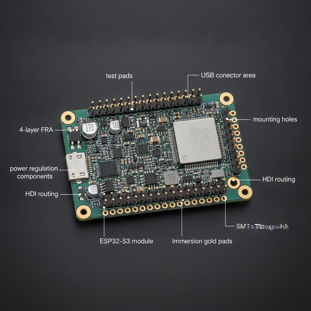
Visible and supplied information points to a compact rectangular board with rounded corners, corner mounting holes, dense surface-mount components, and through-hole headers along the edges. The product data also indicates a 4-layer FR-4 structure with signal, ground, power, and signal layers labeled in the graphic. Immersion gold pads are explicitly stated, and gold-finished contact areas are visible in the imagery.
Capabilities buyers usually evaluate
For this type of board, the important decision factors include layer count, board material, pad finish, assembly density, connector placement, and the ability to support repeatable SMT placement. The stated 4-layer FR-4 HDI PCBA format suggests a manufacturing path intended for more compact routing than a simple single-layer or two-layer design. That said, exact stack-up details, via structure, copper thickness, and impedance control were not provided and should be confirmed before ordering.
Materials and Surface Finish Options
The provided data identifies FR-4 as the base material. FR-4 is widely used in embedded electronics because it balances cost, mechanical rigidity, and manufacturability. The image text also specifies immersion gold, which is commonly chosen when stable solderability and reliable contact surfaces are needed. In practice, an immersion gold PCB assembly is often selected for boards with fine-pitch parts, exposed pads, and connectors that benefit from a clean surface finish.
Other finish choices may exist in custom projects, but they are not confirmed here. Buyers should ask whether the build will use ENIG, HASL, or another finish, and whether the finish is applied across the entire board or only on selected pads and edge contacts.
Manufacturing and Assembly Process
This product falls into the category of PCB fabrication plus PCBA. The workflow typically includes bare board fabrication, solder paste printing, SMT placement, reflow soldering, through-hole insertion where needed, inspection, and test. In a dense board like this one, the placement of the main ESP32S3 device, small passives, power circuitry, USB interface parts, and connectors requires controlled assembly accuracy.
Process steps commonly involved
1) Fabricating the 4-layer FR-4 board
2) Applying surface finish such as immersion gold
3) SMT component placement for ICs, passives, and interface devices
4) Reflow soldering and post-solder inspection
5) Through-hole assembly for headers or connectors
6) Electrical test, visual check, and packaging
When boards are built for OEM projects, DFMA support can help reduce assembly risk by reviewing footprint choices, part spacing, and hand-solder-sensitive locations before production starts.
Application Scenarios
ESP32S3 development board PCBA builds are commonly used in IoT gateways, wireless sensor nodes, smart home controllers, industrial prototypes, automation modules, and embedded software evaluation. They are also useful for device makers who need to validate USB connectivity, power behavior, or antenna-related integration before committing to a final enclosure. Because the ESP32S3 platform is widely used for connected applications, it is often selected for firmware development and product verification runs.
Quality Control and Reliability Considerations
For a custom PCBA, quality control should cover solder joint inspection, polarity verification, connector alignment, and basic electrical continuity checks. If the board is used in development work, consistency matters as much as raw performance. A small defect in a USB connector, header row, or fine-pitch device can interrupt debugging and delay firmware testing.
hcdpcba states that it provides SMT assembly, component sourcing, assembly, testing, and quality control support, along with OEM and ODM services. Buyers should still confirm what inspection methods are included for a specific project, especially if the board will be used in pilot production or field trials.
Customization Guidance for Buyers
Before placing an order, it helps to define the exact board purpose: development kit, validation platform, or production-intent OEM board. From there, specify the layer count, finish preference, connector type, header arrangement, test points, and any mechanical constraints such as mounting hole locations. If the project requires RF or high-speed behavior, ask for stack-up review and layout guidance early. For mixed prototype and production use, it is also useful to align component sourcing and test coverage at the quotation stage.
Questions to confirm with the factory
Can the board be built as a 4-layer FR-4 HDI PCBA with immersion gold? Are SMT and through-hole assembly both included? Is component procurement available? What electrical tests are performed? Can the design be adjusted for OEM branding, connector changes, or enclosure fit?
Why Work with hcdpcba
hcdpcba offers PCB prototyping, SMT assembly, component sourcing, testing, DFMA support, and OEM/ODM services. For buyers who need a reliable build path for an ESP32S3 development board, that combination can simplify project management and reduce the number of vendors involved. The company also states support for multilayer boards, HDI boards, and high-frequency boards, which is relevant when a design moves beyond a simple demo board into a denser custom embedded product.
Contact and Next Step
If you are sourcing an ESP32S3 development board PCBA for prototyping or OEM integration, send the schematic, BOM, Gerbers, and assembly requirements for review. Early DFMA feedback can help avoid footprint conflicts, connector issues, and test problems later in the build. For direct discussion, contact hcdpcba at +86 18924624188 to confirm manufacturability, assembly scope, and customization options for your project.