Product Overview
A Loaded Printed Circuit Board is the practical answer when a buyer needs more than a bare PCB and wants a board that is already populated, soldered, and ready for downstream inspection or system integration. The assembly shown here appears to be a compact control or interface board with dense SMT placement, multiple connectors, and mounting holes, which makes it suitable for embedded electronics, industrial modules, prototyping, or subassemblies inside finished devices. For teams trying to reduce assembly steps and shorten bring-up time, a finished board like this can remove a major sourcing and soldering burden.
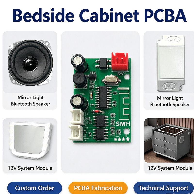
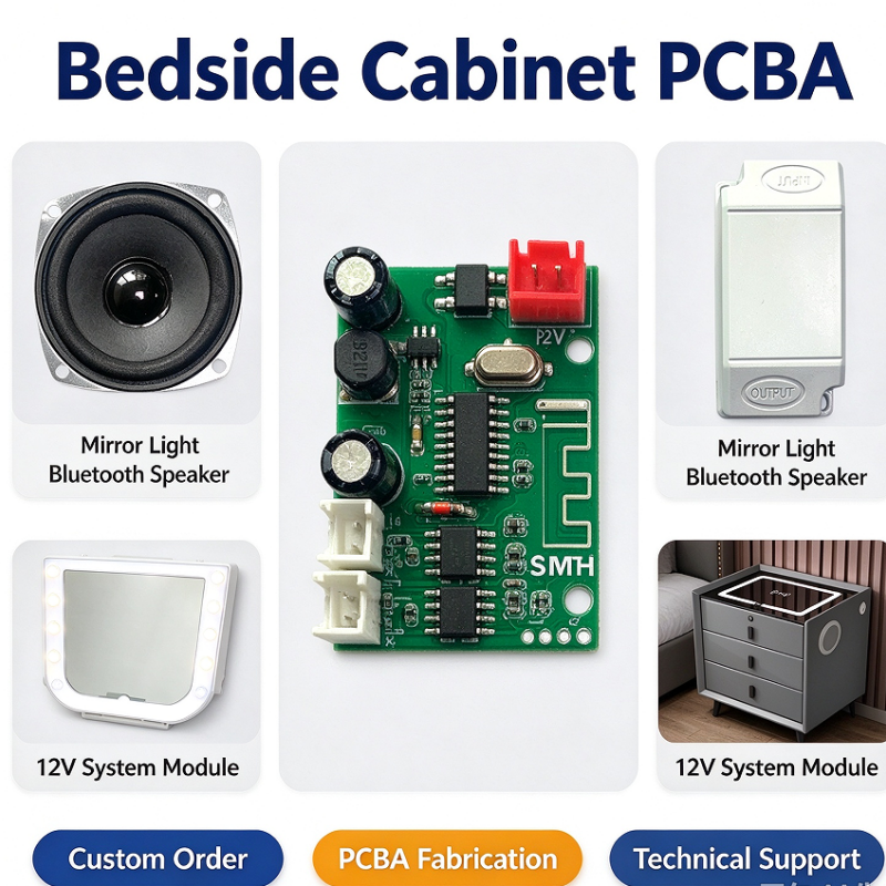
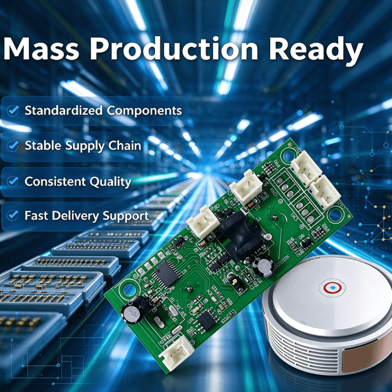
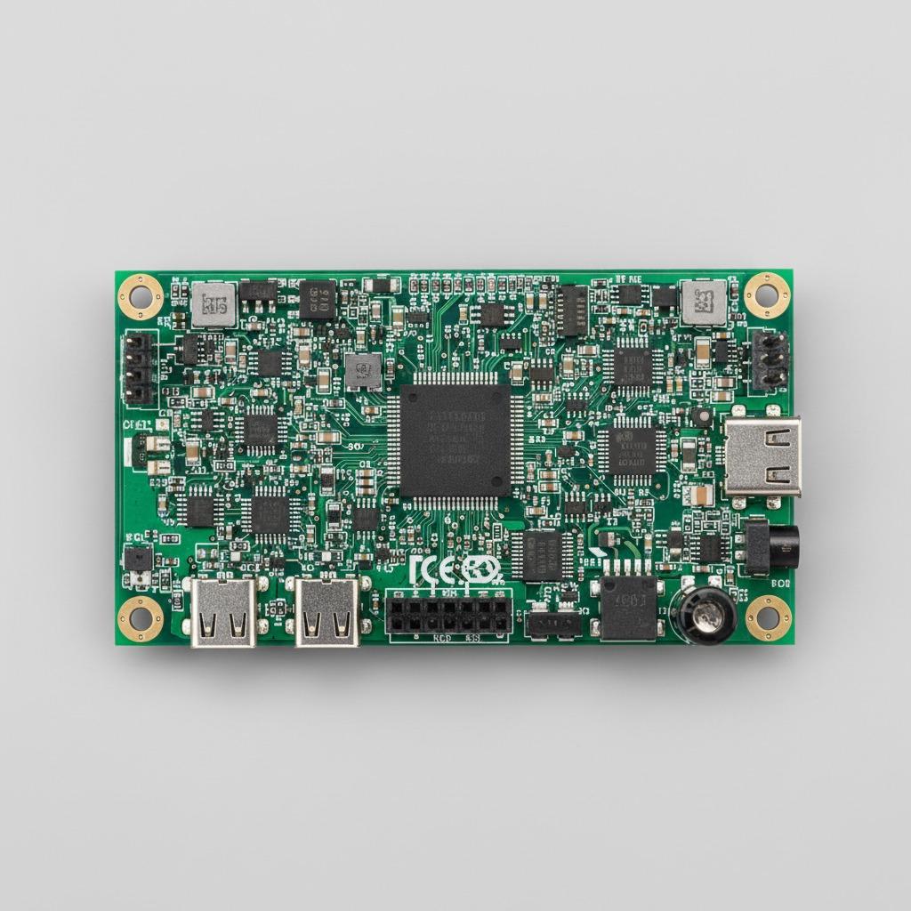
Based on the visible structure, this board is a fully assembled electronics module rather than a bare substrate. The layout includes a central main IC, several smaller support devices, passives, headers, and at least one USB-type connector. That combination suggests a board designed to handle signal processing, communication, or control tasks, although the exact end function cannot be identified from the image alone.
Visible Construction And Capabilities
The board appears to use a rigid FR-4-style laminate with a green solder mask and silkscreen markings. The component side is densely populated, and the layout indicates surface-mount assembly with a mix of fine-pitch ICs, small passives, crystal or oscillator support, and I/O connectors. The visible mounting holes at the corners support mechanical fixing inside a housing, fixture, or larger enclosure.
From a buyer’s perspective, the most useful visible capabilities are straightforward: the board is already assembled, the components are soldered in place, and the interconnect points are in position for system-level wiring or testing. That makes this style of Loaded PCB Assembly useful for engineering samples, pilot builds, and production subassemblies where board-level work has already been completed.
What Can Be Inferred Safely
The image shows a high-density SMT layout, exposed copper/contact areas at connectors, and a board shape that favors compact device integration. The board looks suitable for electrical validation after assembly, but exact test coverage, firmware status, and performance limits are not visible and should not be assumed.
Materials And Finish Options
The visible finish looks consistent with a green solder-mask PCB, likely on FR-4 fiberglass. Exposed metal is visible on connector pads, mounting holes, and contact areas, which is typical for boards that need reliable solderability and mechanical fastening. The overall finish appears functional rather than decorative, which is exactly what most OEM buyers want from a Populated PCB Board.
In custom projects, finish decisions are usually driven by assembly method, connector wear, environment, and budget. For example, surface finish choices, solder mask color, copper thickness, and silkscreen detail can all be adapted to the application. Because those details are not visible here, they should be treated as configurable options rather than confirmed specifications.
Manufacturing Process
This kind of SMT Loaded PCB Board is typically produced through a sequence that includes PCB fabrication, solder paste printing, SMT placement, reflow soldering, and inspection. If through-hole parts are used, they are usually installed in a later insertion and soldering step. The visible board suggests a process focused on fine-pitch component placement and controlled soldering quality, especially around the central IC and the surrounding support devices.
For contract manufacturing buyers, the value is not only in placing parts, but in keeping the whole assembly process consistent across small or large runs. Hcdpcba offers SMT贴片, PCBA板, PCB打样, 元器件代采, 组装, 测试, and DFMA support, so the service model fits projects that need both assembly and manufacturing feedback during development.
Application Scenarios
Although the exact end product is not identifiable from the image, the board style fits a wide range of electronics work. Common use cases include industrial control modules, communications hardware, embedded systems, prototype validation boards, and internal subassemblies for consumer or commercial devices. The presence of multiple connectors also suggests a board meant to bridge signals between subsystems or external interfaces.
For engineering teams, a populated printed circuit board can be especially useful when the design must be tested as a functional unit before final enclosure integration. It also helps when the BOM is complex and the buyer wants one supplier to coordinate sourcing, assembly, and test.
Quality Control Considerations
The image and supplied notes indicate an inspected assembly theme, but exact inspection methods are not confirmed. In practice, a reliable PCBA program normally uses visual inspection, solder quality review, and functional testing where appropriate. For dense assemblies, attention to component alignment, solder joint consistency, connector seating, and contamination control matters as much as placement accuracy.
Buyers should ask for the actual test flow used on their project. That may include incoming material checks, post-reflow inspection, and electrical verification tailored to the design. Since no specific standard or pass criteria are provided here, any claim beyond visible assembly quality would be speculative.
Customization Guidance
If you are sourcing a Loaded Printed Circuit Board for a new product, start by defining the BOM, expected interfaces, operating environment, and production volume. Those inputs influence layer count, component density, connector selection, and assembly sequence. For some projects, a Populated Printed Circuit Board can be optimized for smaller size and easier routing; for others, thermal behavior, mechanical reinforcement, or serviceability takes priority.
Hcdpcba supports PCB prototyping, SMT assembly, component sourcing, OEM, and ODM service, which makes it easier to move from sample builds to repeatable production. When discussing a custom board, it helps to share Gerber files, pick-and-place data, BOM, polarity notes, test requirements, and any mechanical limits such as enclosure clearance or mounting constraints.
Buyer Decision Factors
Before placing an order, buyers usually compare assembly capability, sourcing support, communication speed, and quality control discipline. For a board like this, the most important questions are whether the supplier can handle the component mix, whether fine-pitch placement is stable, and whether testing matches the product’s risk profile. If your design includes BGA, dense SMT, or mixed connector types, ask early about process control and inspection methods.
It is also worth confirming what is included in the quoted scope: bare board fabrication, SMT assembly, through-hole work, component procurement, and test. Clear scope definition reduces rework and avoids assumptions about part availability or assembly responsibility. That is especially important for a Populated PCB Board that is intended for a production line rather than a one-off lab build.
Contact And Next Step
If you need a Loaded PCB Assembly for prototyping or production, hcdpcba can support PCB fabrication, SMT placement, component sourcing, assembly, and testing under one workflow. Share your drawings, BOM, and target application, and the team can help assess manufacturability and build readiness. For direct contact, the company phone number provided is +86 18924624188.