


In the realm of modern electronics manufacturing, Industrial PCB Assembly stands as a cornerstone for creating reliable and high-performance circuit boards tailored to demanding industrial applications. At hcdpcba, we specialize in delivering top-tier Industrial PCB Assembly services that integrate advanced technologies to ensure precision, durability, and efficiency. Our expertise spans from initial design to final testing, making us a trusted partner for industries like industrial control, medical devices, automotive electronics, and IoT solutions. With a focus on quality and innovation, our Industrial PCB Assembly processes are designed to meet the rigorous standards of today's fast-paced technological landscape, providing clients with circuit boards that power everything from automation systems to smart home devices.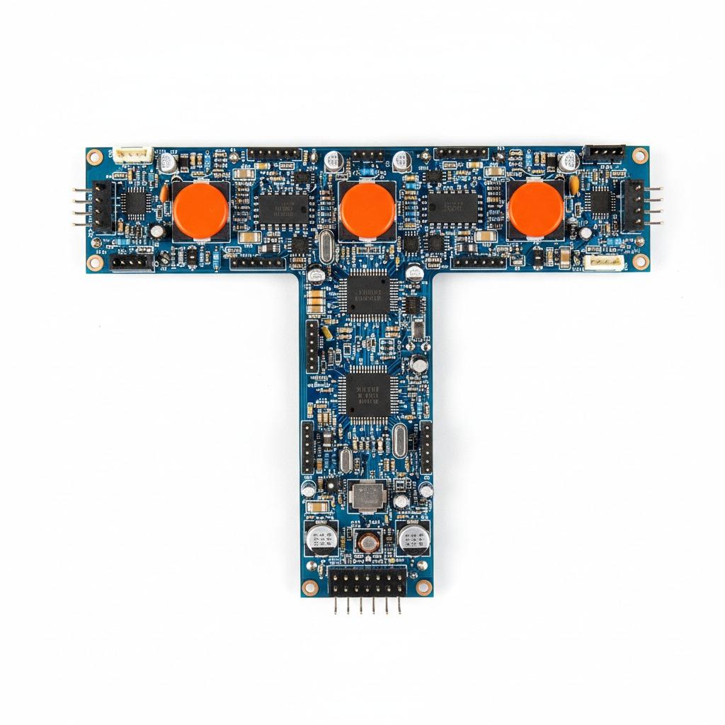
A key aspect of our Industrial PCB Assembly services is the incorporation of Automated Optical Inspection (AOI) in PCB Assembly, which plays a vital role in maintaining impeccable quality control. AOI in PCB Assembly utilizes high-resolution cameras and sophisticated algorithms to detect defects such as soldering issues, component misplacements, and trace errors in real-time. This non-contact method enhances the accuracy of inspections, reducing human error and accelerating production cycles. At hcdpcba, our state-of-the-art AOI systems are integrated into the assembly line, allowing for immediate feedback and corrections that minimize rework and downtime. By leveraging AOI in PCB Assembly, we ensure that every board meets stringent specifications, contributing to higher yields and lower costs for our clients. This technology is particularly invaluable in high-volume production environments where consistency is paramount, and our team of experienced engineers fine-tunes these systems to align with specific project requirements, whether for multi-layer HDI boards or high-frequency applications.
Complementing our inspection capabilities is Flying Probe Testing for PCBs, an advanced method that offers unparalleled flexibility in electrical testing without the need for custom test fixtures. Flying Probe Testing for PCBs employs movable probes to make direct contact with test points on the board, verifying continuity, shorts, and component values with pinpoint accuracy. This approach is ideal for low to medium volume runs, prototypes, and complex boards where traditional bed-of-nails testing falls short. hcdpcba's implementation of Flying Probe Testing for PCBs allows us to handle intricate designs efficiently, supporting rapid prototyping through our PCB打样 services. The system's programmability enables quick adaptations to varying board layouts, ensuring comprehensive coverage of nets and components. In practice, this means faster time-to-market for our clients, as we can identify and resolve issues early in the development phase. Our Flying Probe Testing for PCBs is backed by comprehensive data analysis, providing detailed reports that help optimize designs via our DFMA services, ultimately enhancing product reliability in sectors like communications, power systems, and artificial intelligence.
Beyond these core technologies, hcdpcba's Industrial PCB Assembly encompasses a full suite of services including SMT贴片 for precise component placement, 元器件代采 for sourcing authentic parts, and thorough组装与测试 to guarantee performance. Our OEM and ODM offerings allow for customized solutions, from concept to delivery, with a commitment to confidentiality and cost-effectiveness. Serving diverse applications in安防, 电力, and智能家居, we pride ourselves on our rapid response times and zero-defect quality assurance. Whether you're a startup needing quick prototypes or an enterprise scaling production, our Industrial PCB Assembly expertise ensures your projects succeed with technological precision and professional support. Contact us at +86 18924624188 to discuss how we can elevate your electronics manufacturing needs.

People who viewed this also viewed

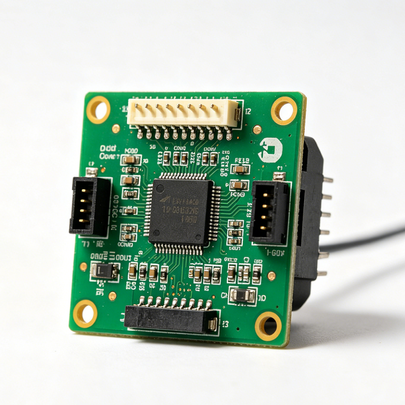
1. Industrial Transmitter PCBA for Compact Industrial Measurement and Interface Modules 2. Product Overview 3. Key Specifications and Visible Capabilities 4. Materials and Finish Options 5. Manufacturing and Assembly Process 6. Application Scenarios 7. Quality Control and Integration Considerations 8. Customization Guidance for Buyers 9. Why Buyers Choose This Type of PCBA 10. Request Custom PCB Assembly Support

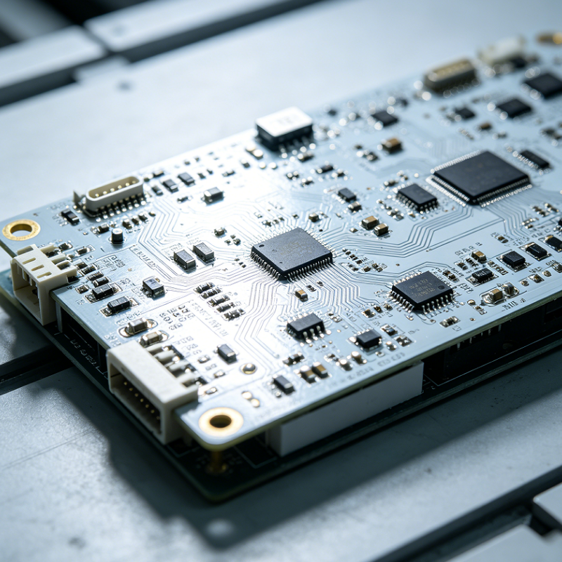
1. Industrial Lighting Control PCBA for Reliable Embedded Control 2. Product Overview 3. Key Capabilities and Design Features 4. Materials and Finish Options 5. Manufacturing Process 6. Typical Application Scenarios 7. Quality Control Considerations 8. Customization Guidance for Buyers 9. Why Buyers Choose a Board-Level Solution 10. Contact for Custom PCBA Projects

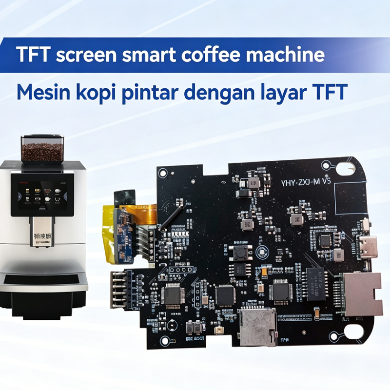
1. coffee machine pcba for smart beverage equipment 2. Product overview 3. Key visible features and capabilities 4. Materials and finish options 5. Manufacturing and assembly process 6. Typical application scenarios 7. Quality control and buyer concerns 8. Customization guidance 9. Choosing the right board for your project 10. Request OEM or ODM support

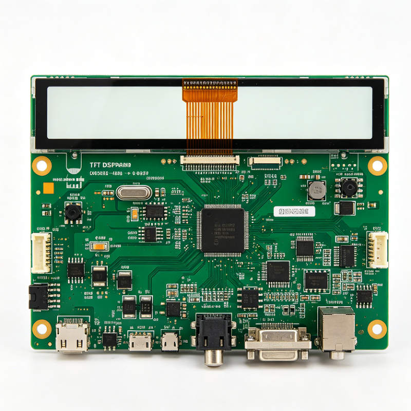
1. TFT Screen Driver Board Overview 2. Product Structure and Visible Features 3. Key Capabilities Buyers Usually Need 4. Materials and Finish Options 5. Manufacturing Process 6. Application Scenarios 7. Quality Control and Assembly Considerations 8. Customization Guidance for OEM Buyers 9. How to Decide If This Board Fits Your Project 10. Contact for Custom PCB Assembly